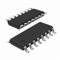
SI3000-C-FS Silicon Laboratories Inc, SI3000-C-FS Datasheet - Page 6

SI3000-C-FS
Manufacturer Part Number
SI3000-C-FS
Description
IC VOICE CODEC 3.3V/5V 16SOIC
Manufacturer
Silicon Laboratories Inc
Type
Voice-Band Codecr
Datasheet
1.SI3000-C-FS.pdf
(34 pages)
Specifications of SI3000-C-FS
Package / Case
16-SOIC (0.154", 3.90mm Width)
Data Interface
Serial
Resolution (bits)
16 b
Number Of Adcs / Dacs
1 / 1
Sigma Delta
No
Dynamic Range, Adcs / Dacs (db) Typ
84 / 84
Voltage - Supply, Analog
3 V ~ 5.25 V
Voltage - Supply, Digital
3 V ~ 5.25 V
Operating Temperature
0°C ~ 70°C
Mounting Type
Surface Mount
Number Of Adc Inputs
3
Number Of Dac Outputs
2
Conversion Rate
12 KSPs
Resolution
16 bit
Maximum Operating Temperature
+ 70 C
Mounting Style
SMD/SMT
Minimum Operating Temperature
0 C
Number Of Channels
1 ADC, 1 DAC
Single Supply Voltage (typ)
3.3/5V
Single Supply Voltage (min)
3V
Single Supply Voltage (max)
5.25V
Lead Free Status / RoHS Status
Lead free / RoHS Compliant
Lead Free Status / RoHS Status
Lead free / RoHS Compliant, Lead free / RoHS Compliant
Other names
336-1382
SI3000-C-FS
SI3000-C-FS
Available stocks
Company
Part Number
Manufacturer
Quantity
Price
Company:
Part Number:
SI3000-C-FS
Manufacturer:
Exar
Quantity:
40
Part Number:
SI3000-C-FS
Manufacturer:
SILICON LABS/芯科
Quantity:
20 000
Company:
Part Number:
SI3000-C-FSR
Manufacturer:
SILICON
Quantity:
17 315
Table 4. AC Characteristics (Continued)
(V
Table 5. Absolute Maximum Ratings
Si3000
6
Parameter
DAC Output Gain Step Size
DAC Freq Response
DAC Freq Response
DAC Freq Response
DAC Line Output Load Resistance
DAC Line Output Load Capacitance
DAC SPKR Output Load Resistance
DAC Gain Drift
Interchannel Isolation (Crosstalk)
HDST Full Scale Level Input
HDST Full Scale Level Output
HDST Output Resistance
MIC Bias Voltage
MIC Power Supply Rejection Ratio
Notes:
Parameter
DC Supply Voltage
Input Current, Si3000 Digital Input Pins
Digital Input Voltage
Operating Temperature Range
Storage Temperature Range
Note: Permanent device damage may occur if the above Absolute Maximum Ratings are exceeded. Functional operation
A
, V
1. DR = VIN + 20 log (RMS signal/RMS noise). Measurement bandwidth is 300 to 3400 Hz. Valid sample rate ranges
2. 0 dB setting for analog and digital attenuation/gain.
3. THD = 20 log (RMS distortion/RMS signal). Valid sample rate ranges between 4000 and 12000 Hz.
4. At 0 dB gain setting, 1 V
5. These characteristics are determined by external components. See Figure 13.
6. With a 600 load. Output starts clipping with half of full scale digital input, which corresponds to a 0.5 V
D
= 5 V ±5% or 3.3 V ±10%, T
between 4000 and 12000 Hz.
should be restricted to the conditions as specified in the operational sections of this data sheet. Exposure to absolute
maximum rating conditions for extended periods may affect device reliability.
5
5
6
rms
input corresponds to –1.5 dB of full scale digital output code.
A
= 0 to 70°C)
Symbol
V
PSRR
Rout
F
F
F
mbias
A
RR
RR
RR
T
Symbol
V
T
V
D
Low –3 dB corner
Rev. 1.4
I
T
STG
IND
Test Condition
IN
, V
A
VIN = 1 kHz
A
3400 Hz
300 Hz
DC
–0.3 to (V
–0.5 to 6.0
–10 to 100
–40 to 150
Value
±10
–0.01
–0.2
Min
600
D
—
—
—
—
—
—
—
—
—
—
—
+ 0.3)
0.002
Typ
600
1.5
0.5
1.0
2.5
33
60
90
40
—
—
—
—
Max
40
—
—
—
—
—
—
—
—
—
—
—
0
0
rms
Unit
mA
°C
°C
V
V
output.
dB/°C
Unit
V
V
dB
Hz
dB
dB
dB
dB
pF
rms
rms
V


