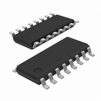
SI3000-C-FS Silicon Laboratories Inc, SI3000-C-FS Datasheet - Page 31

SI3000-C-FS
Manufacturer Part Number
SI3000-C-FS
Description
IC VOICE CODEC 3.3V/5V 16SOIC
Manufacturer
Silicon Laboratories Inc
Type
Voice-Band Codecr
Datasheet
1.SI3000-C-FS.pdf
(34 pages)
Specifications of SI3000-C-FS
Package / Case
16-SOIC (0.154", 3.90mm Width)
Data Interface
Serial
Resolution (bits)
16 b
Number Of Adcs / Dacs
1 / 1
Sigma Delta
No
Dynamic Range, Adcs / Dacs (db) Typ
84 / 84
Voltage - Supply, Analog
3 V ~ 5.25 V
Voltage - Supply, Digital
3 V ~ 5.25 V
Operating Temperature
0°C ~ 70°C
Mounting Type
Surface Mount
Number Of Adc Inputs
3
Number Of Dac Outputs
2
Conversion Rate
12 KSPs
Resolution
16 bit
Maximum Operating Temperature
+ 70 C
Mounting Style
SMD/SMT
Minimum Operating Temperature
0 C
Number Of Channels
1 ADC, 1 DAC
Single Supply Voltage (typ)
3.3/5V
Single Supply Voltage (min)
3V
Single Supply Voltage (max)
5.25V
Lead Free Status / RoHS Status
Lead free / RoHS Compliant
Lead Free Status / RoHS Status
Lead free / RoHS Compliant, Lead free / RoHS Compliant
Other names
336-1382
SI3000-C-FS
SI3000-C-FS
Available stocks
Company
Part Number
Manufacturer
Quantity
Price
Company:
Part Number:
SI3000-C-FS
Manufacturer:
Exar
Quantity:
40
Part Number:
SI3000-C-FS
Manufacturer:
SILICON LABS/芯科
Quantity:
20 000
Company:
Part Number:
SI3000-C-FSR
Manufacturer:
SILICON
Quantity:
17 315
7. 16-Pin SOIC Land Pattern
Figure illustrates the recommended land pattern for the Si3000 16-pin SOIC. Table 16 lists the values for the
dimensions shown in the illustration.
Notes:
General
Solder Mask Design
Stencil Design
Card Assembly
Dimension
1. All dimensions shown are in millimeters (mm) unless otherwise noted.
2. Dimensioning and Tolerancing per ASME Y14.5M-1994.
3. This Land Pattern Design is based on the IPC-7351 guidelines.
4. All dimensions shown are at Maximum Material Condition (MMC). Least Material Condition (LMC) is calculated based on a
5. All metal pads are to be non-solder mask defined (NSMD). Clearance between the solder mask and the metal pad is to be 60 µm
6. A stainless steel, laser-cut and electro-polished stencil with trapezoidal walls should be used to assure good solder paste release.
7. The stencil thickness should be 0.125 mm (5 mils).
8. The ratio of stencil aperture to land pad size should be 1:1.
9. A No-Clean, Type-3 solder paste is recommended.
10. The recommended card reflow profile is per the JEDEC/IPC J-STD-020 specification for Small Body Components.
Fabrication Allowance of 0.05 mm.
minimum, all the way around the pad.
C1
X1
Y1
E
Table 16. 16-Pin MSOP Land Pattern Dimensions
Figure 20. 16-Pin SOIC Land Pattern Diagram
Pad Column Spacing
Pad Row Pitch
Rev. 1.4
Pad Length
Pad Width
Feature
Si3000
5.40
1.27
0.60
1.55
mm
31


