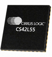
CS42L55-DNZ Cirrus Logic Inc, CS42L55-DNZ Datasheet - Page 68

CS42L55-DNZ
Manufacturer Part Number
CS42L55-DNZ
Description
IC CODEC STER H-HDPN AMP 36-QFN
Manufacturer
Cirrus Logic Inc
Type
Stereo Audior
Datasheet
1.CS42L55-CNZ.pdf
(73 pages)
Specifications of CS42L55-DNZ
Data Interface
Serial
Resolution (bits)
24 b
Number Of Adcs / Dacs
1 / 1
Sigma Delta
Yes
Dynamic Range, Adcs / Dacs (db) Typ
95 / 99
Voltage - Supply, Analog
1.65 V ~ 2.71 V
Voltage - Supply, Digital
1.65 V ~ 2.71 V
Operating Temperature
-40°C ~ 85°C
Mounting Type
Surface Mount
Package / Case
36-QFN
Lead Free Status / RoHS Status
Lead free / RoHS Compliant
For Use With
598-1506 - BOARD EVAL FOR CS42L55 CODEC
Lead Free Status / RoHS Status
Lead free / RoHS Compliant, Lead free / RoHS Compliant
68
7. PCB LAYOUT CONSIDERATIONS
7.1
7.2
7.3
Power Supply
As with any high-resolution converter, the CS42L55 requires careful attention to power supply and ground-
ing arrangements if its potential performance is to be realized.
ed power arrangements, with VA and VCP connected to clean supplies. VLDO, which powers the digital
circuitry, may be run from the system logic supply. Alternatively, VLDO may be powered from the analog
supply via a ferrite bead. In this case, no additional devices should be powered from VLDO.
Grounding
Extensive use of power and ground planes, ground plane fill in unused areas and surface mount decoupling
capacitors are recommended. Decoupling capacitors should be as close to the pins of the CS42L55 as pos-
sible. The low value ceramic capacitor should be closest to the pin and should be mounted on the same
side of the board as the CS42L55 to minimize inductance effects. All signals, especially clocks, should be
kept away from the FILT+ and VQ pins in order to avoid unwanted coupling into the modulators. The FILT+,
VQ, +VHPFILT and -VHPFILT capacitors must be positioned to minimize the electrical path from each re-
spective pin to AGND. The CDB42L55 evaluation board demonstrates the optimum layout and power sup-
ply arrangements.
QFN Thermal Pad
The CS42L55 comes in a compact QFN package. The under side of the QFN package reveals a large metal
pad that serves as a thermal relief to provide for maximum heat dissipation. This pad must mate with an
equally dimensioned copper pad on the PCB and must be electrically connected to ground. A series of vias
should be used to connect this copper pad to one or more larger ground planes on other PCB layers. In split
ground systems, it is recommended that this thermal pad be connected to AGND for best performance. The
CDB42L55 evaluation board demonstrates the optimum thermal pad and via configuration.
Figure 1 on page 10
shows the recommend-
CS42L55
DS773F1


