LPC47B272-MS SMSC, LPC47B272-MS Datasheet
LPC47B272-MS
Specifications of LPC47B272-MS
Available stocks


Related parts for LPC47B272-MS


LPC47B272-MS Summary of contents
Page 1
... System Management Interrupt • 2.88MB Super I/O Floppy Disk Controller - Licensed CMOS 765B Floppy Disk Controller - Software and Register Compatible with SMSC's Proprietary 82077AA Compatible Core - Supports Two Floppy Drives Directly - Configurable Open Drain/Push-Pull Output Drivers - Supports Vertical Recording Format ...
Page 2
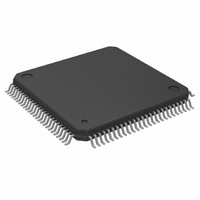
... LPC47B272QFP for 100 pin QFP package LPC47B272-MS for 100 pin QFP Lead-Free RoHS Compliant Package 80 ARKAY DRIVE, HAUPPAUGE, NY 11788 (631) 435-6000, FAX (631) 273-3123 Copyright © 2007 SMSC or its subsidiaries. All rights reserved. Circuit diagrams and other information relating to SMSC products are included as a means of illustrating typical applications. Consequently, complete information sufficient for construction purposes is not necessarily given ...
Page 3
... INSTRUCTION SET .................................................................................................................................................38 FDC SWAP BIT ........................................................................................................................................................54 SERIAL PORT (UART) ...........................................................................................................................................55 INFRARED INTERFACE........................................................................................................................................ ...................................................................................................................................................68 RANSMIT INS MPU-401 MIDI UART..............................................................................................................................................69 O ................................................................................................................................................................69 VERVIEW H I ......................................................................................................................................................69 OST NTERFACE MPU-401 C C OMMAND ONTROLLER MIDI UART.............................................................................................................................................................72 MPU-401 C R ONFIGURATION EGISTERS SMSC LPC47B27x TABLE OF CONTENTS R ............................................................................................12 ULLUP ESISTORS ........................................................................................................................14 ...........................................................................................................................15 .........................................................................................................................72 .................................................................................................................... DATASHEET Rev. 04-17-07 ...
Page 4
... OWER ONTROL EGISTER VREF P ..............................................................................................................................................................125 IN ISA IRQ TO SERIAL IRQ CONVERSION CAPABILITY ...............................................................................126 RUNTIME REGISTERS ........................................................................................................................................127 CONFIGURATION ................................................................................................................................................150 OPERATIONAL DESCRIPTION.........................................................................................................................167 MAXIMUM GUARANTEED RATINGS*............................................................................................................167 DC ELECTRICAL CHARACTERISTICS..........................................................................................................167 TIMING DIAGRAMS ..............................................................................................................................................170 SMSC LPC47B27x IRQ ..........................................................................................................105 S ..........................................................................................................106 C .......................................................................................................123 ONTROL - 4 - DATASHEET Rev. 04-17-07 ...
Page 5
... FIGURE 31 – JOYSTICK POSITION SIGNAL ................................................................................................189 PACKAGE OUTLINE............................................................................................................................................193 APPENDIX - TEST MODE....................................................................................................................................194 ...............................................................................................................................................194 OARD EST ODE SMSC LPC47B27x - 5 - DATASHEET Rev. 04-17-07 ...
Page 6
... The SMSC advanced digital data separator incorporates SMSC's patented data separator technology, allowing for ease of testing and use. Both on- chip UARTs are compatible with the NS16C550A. The parallel port is compatible with IBM PC/AT architecture, as well as IEEE 1284 EPP and ECP ...
Page 7
... GP42/nIO_PME 17 VTR 18 CLOCKI 19 LAD0 20 LAD1 21 LAD2 22 LAD3 23 nLFRAME 24 nLDRQ 25 nPCI_RESET 26 nLPCPD 27 GP43/DDRC/FDC_PP 28 PCI_CLK 29 SER_IRQ 30 SMSC LPC47B27x PIN CONFIGURATION LPC47B27x 100 PIN QFP - 7 - DATASHEET 80 nACK 79 BUSY SLCT 76 VSS 75 PD7 74 PD6 73 PD5 72 PD4 71 PD3 70 PD2 PD1 69 68 PD0 67 nSLCTIN 66 nINIT ...
Page 8
... Read Disk Data 11 Write Gate 10 Write Disk Data 12 Head Select 8 Step Direction 9 Step Pulse 4 Disk Change 5 Drive Select 0 3 Motor Write Protected SMSC LPC47B27x DESCRIPTION OF PIN FUNCTIONS BUFFER TOTAL SYMBOL PROCESSOR/HOST LPC INTERFACE (10) 4 LAD[3:0] PCI_IO 1 nLFRAME PCI_I 1 nLDRQ PCI_O 1 nPCI_RESE PCI_I T ...
Page 9
... I/O/Data Carrier Detect 2/IRQ4 92 General Purpose I/O/Ring Indicator 2/IRQ3 66 Initiate Output/FDC Direction Control 67 Printer Select Input/FDC Step Pulse 68 Port Data 0/FDC Index 69 Port Data 1/FDC Track 0 SMSC LPC47B27x DESCRIPTION OF PIN FUNCTIONS BUFFER TYPE TOTAL SYMBOL 1 nTRKO IS 1 nINDEX IS 1 GP40/ IO12 DRVDEN0 1 ...
Page 10
... General Purpose I/O /Joystick 2 Button 2 36 General Purpose I/O /Joystick 1 X-Axis 37 General Purpose I/O /Joystick 1 Y-Axis 38 General Purpose I/O /Joystick 2 X-Axis 39 General Purpose I/O /Joystick 2 Y-Axis SMSC LPC47B27x DESCRIPTION OF PIN FUNCTIONS BUFFER TYPE TOTAL SYMBOL 1 PD2 IS/OP14 /nWRTPRT 1 PD3 IS/OP14 /nRDATA ...
Page 11
... POR). If the nKBDRST and A20M functions are to be used, the system must ensure that these pins are high. See Section “Pins That Require External Pullup Resistor”. Note 11: The LED pins are powered by VTR so that the LEDs can be controlled when the part is under VTR power SMSC LPC47B27x DESCRIPTION OF PIN FUNCTIONS BUFFER ...
Page 12
... Open Drain Output • nWDATA if used as Open Drain Output • nWGATE if used as Open Drain Output • nHDSEL if used as Open Drain Output • nINDEX • nTRK0 • nWRTPRT • nRDATA • nDSKCHG • GP50-GP57 if the IRQx functions are used SMSC LPC47B27x - 12 - DATASHEET Rev. 04-17-07 ...
Page 13
... PCI Bus Power Management Interface Specification, Rev. 1.0, Draft, March 18, 1997. 5. Low Pin Count (LPC) Interface Specification, Revision 1.0, September 29, 1997, Intel Document. 6. SMSC Application Note, AN 8-8: Using the Enhanced Keyboard and Mouse Wakeup Feature in SMSC Super I/O Parts. 7. SMSC Application Note, AN 9-3: Application Considerations When Using the Powerdown Feature of SMSC Floppy Disk Controllers ...
Page 14
... PLL PME CONTROL POWER (CR24.1) (CR22. SMSC LPC47B27x ) to provide sleep current for the programmable wake-up events in the TR can be connected powers the Consumer IR receiver, IR interface begins a power-on cycle. When V is powered. See Trickle Power Functionality section. TR INTERNAL PWRGOOD X All PLLs Powered Down ...
Page 15
... Hard Reset. GP53 cannot be used for wakeup under VTR power since this is the TXD2(IRTX) pin which comes up as output and low following a VTR POR, a VCC POR and Hard Reset. GP43 reverts to the basic GPIO function when VCC is removed from the part, but its programmed input/output, invert/non-invert and output buffer type is retained. SMSC LPC47B27x - 15 - DATASHEET Rev. 04-17-07 ...
Page 16
... The total maximum current for the part is the unloaded value PLUS the maximum current sourced by the pin that is driven by VTR. The pins that are powered by VTR are as follows: GP42 / nIO_PME, IRTX2 / GP35, GP53/TXD2, GP60 / LED1, GP61 / LED2. These pins, if configured as push-pull outputs, will source a minimum of 6mA at 2.4V when driving. SMSC LPC47B27x - 16 - DATASHEET Rev. 04-17-07 ...
Page 17
... The LPC47B27x offers support for Power Management Events (PMEs), also referred to as System Control Interrupt (SCI) events. The terms PME and SCI are used synonymously throughout this document to refer to the indication of an event to the chipset via the assertion of the nIO_PME output signal on pin 17. See the “PME Support” section. SMSC LPC47B27x - 17 - DATASHEET ...
Page 18
... LPC interface. SER_IRQ I/O Serial IRQ. PCI_CLK Input PCI Clock. Note: The nCLKRUN signal is not implemented in this part. SMSC LPC47B27x FUNCTIONAL DESCRIPTION Table 1 - Super I/O Block Addresses LOGICAL BLOCK NAME DEVICE Floppy Disk Serial Port Com 1 Serial Port Com 2 ...
Page 19
... DMA on the LPC bus is handled through the use of the nLDRQ lines from the LPC47B27x and special encodings on LAD[3:0] from the host. The DMA mechanism for the LPC bus is described in the Low Pin Count (LPC) Interface Specification Revision 1.0. SMSC LPC47B27x Transfer Size 1 Byte ...
Page 20
... In the case of multiple byte cycles, such as DMA cycles, an error SYNC terminates the cycle. Therefore, if the host is transferring 4 bytes from a device, if the device returns the error SYNC in the first byte, the other three bytes will not be transferred. SMSC LPC47B27x This is used for EPP data transfers and should utilize the same timeout - 20 - DATASHEET Rev ...
Page 21
... The LPC47B27x inserts three wait states for a DMA read and four wait states for a DMA write cycle. A SYNC of 0101 is used for all DMA transfers. See the example timing for the LPC cycles in the “Timing Diagrams” section. SMSC LPC47B27x - 21 - DATASHEET Rev. 04-17-07 ...
Page 22
... Selection logic for an IBM XT/AT compatible FDC. The true CMOS 765B core guarantees 100% IBM PC XT/AT compatibility in addition to providing data overflow and underflow protection. The FDC is compatible to the 82077AA using SMSC's proprietary floppy disk controller core. FDC INTERNAL REGISTERS The Floppy Disk Controller contains eight internal registers which facilitate the interfacing between the host microprocessor and the disk drive ...
Page 23
... PS/2 Mode RESET 1 1 COND. BIT 0 MOTOR ENABLE 0 Active high status of the MTR0 disk interface output pin. This bit is low after a hardware reset and unaffected by a software reset. SMSC LPC47B27x STEP TRK0 nHDSEL INDX F N/A 1 ...
Page 24
... BIT 5 nDRIVE SELECT 0 Active low status of the DS0 disk interface output. BIT 6 nDRIVE SELECT 1 Active low status of the DS1 disk interface output. BIT 7 nDRV2 Active low status of the DRV2 disk interface input. Note: This function is not supported. SMSC LPC47B27x nDS0 WDATA ...
Page 25
... BIT 6 MOTOR ENABLE 2 The MTR2 disk interface output is not supported in the LPC47B27x. BIT 7 MOTOR ENABLE 3 The MTR3 disk interface output is not supported in the LPC47B27x. DIGITAL OUTPUT REGISTER Bit 5 Bit 4 Bit1 SMSC LPC47B27x MOT MOT DMAEN nRESE EN1 EN0 DRIVE DOR VALUE 0 ...
Page 26
... This register is write only used to program the data rate, amount of write precompensation, power down status, and software reset. The data rate is programmed using the Configuration Control Register (CCR) not the DSR, for PC/AT and PS/2 Model 30. SMSC LPC47B27x DRIVE SELECT OUTPUTS (ACTIVE LOW) ...
Page 27
... DRIVE RATE DRT1 DRT0 SEL1 SMSC LPC47B27x PRE- PRE- PRE- COMP2 COMP1 COMP0 Table 7 - Precompensation Delays PRECOMPENSATION DELAY (nsec) <2Mbps 0.00 41.67 83.34 125.00 166.67 208.33 250.00 Default Default: See Table 10 Table 8 - Data Rates ...
Page 28
... Reserved, read ‘0’. This part does not support non-DMA mode. BIT 6 DIO Indicates the direction of a data transfer once a RQM is set indicates a read and a 0 indicates a write is required. BIT 7 RQM Indicates that the host can transfer data if set access is permitted if set SMSC LPC47B27x DATA RATE DATA RATE SEL0 MFM ...
Page 29
... DSK 0 CHG RESET N/A N/A COND. SMSC LPC47B27x Table 11 - FIFO Service Delay MAXIMUM DELAY TO SERVICING AT 2 Mbps DATA RATE µs - 1.5 µs = 2.5 µ µs - 1.5 µs = 6.5 µ µs - 1.5 µs = 30.5 µ µs - 1.5 µs = 58.5 µs MAXIMUM DELAY TO SERVICING AT 1 Mbps DATA RATE µ ...
Page 30
... BITS UNDEFINED Always read as a logic "0" BIT 7 DSKCHG This bit monitors the pin of the same name and reflects the opposite value seen on the disk cable or the value programmed in the Force Disk Change Register (see Runtime Register at offset 0x1E). SMSC LPC47B27x ...
Page 31
... STATUS REGISTER ENCODING During the Result Phase of certain commands, the Data Register contains data bytes that give the status of the command just executed. BIT NO. SYMBOL NAME 7,6 IC Interrupt Code 00 - Normal termination of command Seek End 4 EC Equipment Check SMSC LPC47B27x N/A N/A N/A N ...
Page 32
... SYMBOL NAME Write Protected 5 SMSC LPC47B27x DESCRIPTION Unused. This bit is always "0". The current selected drive. Table 13 - Status Register 1 DESCRIPTION The FDC tried to access a sector beyond the final sector of the track (255D). Will be set not issued after Read or Write Data command. ...
Page 33
... FDC before the command phase is complete. (Please refer to Table 16 for the command set descriptions). These bytes of data must be transferred in the order prescribed. SMSC LPC47B27x DESCRIPTION Indicates the status of the TRK0 pin. ...
Page 34
... If the last sector to be transferred is a partial sector, the host can stop transferring the data in mid-sector, and the FDC will continue to complete the sector cycle was received. The only difference between these implicit functions and TC cycle is that they return "abnormal termination" result status. Such status indications can be ignored if they were expected. SMSC LPC47B27x - 34 - DATASHEET Rev. 04-17-07 ...
Page 35
... RQM and DIO must both equal "1" before the result bytes may be read. After all the result bytes have been read, the RQM and DIO bits switch to "1" and "0" respectively, and the CB bit is cleared, indicating that the FDC is ready to accept the next command. SMSC LPC47B27x - 35 - DATASHEET ...
Page 36
... With this flag set, a multitrack read or write operation will automatically continue to the first sector under head 1 when the FDC finishes operating on the last sector under head 0. SMSC LPC47B27x COMMAND SET/DESCRIPTIONS DESCRIPTION which ...
Page 37
... ST2 Status 2 the host during the result phase after command execution. ST3 Status 3 WGATE Write Gate Alters timing allow for pre-erase loads in perpendicular drives. SMSC LPC47B27x DESCRIPTION The number of bytes SECTOR SIZE 128 Bytes 256 Bytes 512 Bytes 1024 Bytes … ...
Page 38
... R ──────── R ──────── N ──────── R SMSC LPC47B27x INSTRUCTION SET Table 17 - Instruction Set READ DATA ...
Page 39
... N ──────── R PHASE R Command W MT MFM Execution Result SMSC LPC47B27x WRITE DATA DATA BUS Command Codes HDS DS1 DS0 Sector ID information prior to Command execution. Data transfer between the FDD and system. Status information after Com- mand execution. Sector ID information after Command execution. ...
Page 40
... W Execution Result PHASE R Command Result SMSC LPC47B27x READ A TRACK DATA BUS HDS DS1 DS0 ──────── C ──────── ──────── H ──────── ...
Page 41
... ─── SRT ─── W ────── HLT ────── W PHASE R Command Result R SMSC LPC47B27x FORMAT A TRACK DATA BUS HDS DS1 DS0 ──────── N ──────── ...
Page 42
... D7 D6 Command W 0 Execution Result ──── SRT ──── LOCK R 0 EIS EFIFO R SMSC LPC47B27x SEEK DATA BUS HDS DS1 DS0 ─────── NCN ─────── ...
Page 43
... A set of nine (9) bytes is required to place the FDC in the Read Data Mode. After the Read Data command has been issued, the FDC loads the head ( the unloaded state), waits the specified head settling time (defined in the Specify command), and begins reading ID Address Marks and ID fields. When the sector address read off the diskette SMSC LPC47B27x READ ID DATA BUS ...
Page 44
... Read Data Command. Table 20 describes the effect of the SK bit on the Read Data command execution and results. Except where noted in Table 20, the value of the sector address is automatically incremented (see Table 22 SMSC LPC47B27x Table 18 - Sector Sizes N SECTOR SIZE 00 128 bytes 01 256 bytes 02 512 bytes 03 1024 bytes .. ... 07 16 Kbytes ...
Page 45
... This command terminates when the EOT specified number of sectors has not been read. If the FDC does not find an ID Address Mark on the diskette after the second occurrence of a pulse on the nINDEX pin, then it sets the IC code in Status Register 0 to "01" (abnormal termination), sets the MA bit in Status Register 1 to "1", and terminates the command. SMSC LPC47B27x RESULTS SECTOR CM BIT OF ...
Page 46
... Table 22 and Table 23 for information concerning the values of MT and EC versus SC and EOT value. Definitions: # Sectors Per Side = Number of formatted sectors per each side of the disk. # Sectors Remaining = Number of formatted sectors left which can be read, including side 1 of the disk set to "1". SMSC LPC47B27x Table 22 - Result Phase ID INFORMATION AT RESULT PHASE C H ...
Page 47
... FDC encounters a pulse on the nINDEX pin again and it terminates the command. Table 24 contains typical values for gap fields which are dependent upon the size of the sector and the number of sectors on each track. Actual values can vary due to drive electronics. SMSC LPC47B27x Table 23 - Verify Command Result Phase SC/EOT VALUE Success Termination ...
Page 48
... ID field it is able to read into its registers. If the FDC does not find an ID address mark on the diskette after the second occurrence of a pulse on the nINDEX pin, it then sets the IC code in Status Register 0 to "01" (abnormal termination), sets the MA bit in Status Register 1 to "1", and terminates the command. SMSC LPC47B27x FORMAT FIELDS SYSTEM 34 (DOUBLE DENSITY) FORMAT ...
Page 49
... Format A Track command g. Write Deleted Data command h. Verify command 2. End of Seek, Relative Seek, or Recalibrate command The Sense Interrupt Status command resets the interrupt signal and, via the IC code and SE bit of Status Register 0, identifies the cause of the interrupt. SMSC LPC47B27x - 49 - DATASHEET Rev. 04-17-07 ...
Page 50
... POLL - Polling Enabled FIFOTHR - FIFO Threshold Set to 1 Byte PRETRK - Pre-Compensation Set to Track 0 EIS - Enable Implied Seek. When set to "1", the FDC will perform a Seek operation before executing a read or write command. Defaults to no implied seek. SMSC LPC47B27x Table 25 - Interrupt Identification SE IC INTERRUPT DUE TO ...
Page 51
... This may require the host to issue a Read ID command to ensure that the head is physically on the track that software assumes it to be. Different FDC commands will return different cylinder results which may be difficult to keep track of with software without the Read ID command. SMSC LPC47B27x DIR ACTION ...
Page 52
... DOR or DSR registers) will only clear GAP and WGATE bits to "0". D0-D3 are unaffected and retain their previous value. 2. "Hardware" resets will clear all bits (GAP, WGATE and D0-D3) to "0", i.e all conventional mode. SMSC LPC47B27x - 52 - DATASHEET Rev. 04-17-07 ...
Page 53
... Bit[1] in the Force Disk Change register supports the second floppy. Setting either of the Force Disk Change bits active forces the internal FDD nDSKCHG active when the appropriate drive has been selected. The Force Disk Change register is defined in the Runtime Registers section. SMSC LPC47B27x Table 27 - Effects of WGATE and GAP Bits LENGTH OF ...
Page 54
... FDC SWAP BIT The FDC_SWAP bit in the FDD Mode Register (configuration register 0xF0) can be used to swap Drive 0 and Drive 1. The FDC_SWAP is defined as follows: Bit[4] FDC_SWAP Not Swap (default Swap Drive 0 (nDS, nMTR pins) with Drive 1 (nDS, nMTR pins) SMSC LPC47B27x - 54 - DATASHEET Rev. 04-17-07 ...
Page 55
... Similarly, setting the appropriate bits of this register to a high, selected interrupts can be enabled. Disabling the interrupt system inhibits the SMSC LPC47B27x SERIAL PORT (UART) Table 28 - Addressing the Serial Port ...
Page 56
... Writing to this bit has no effect on the operation of the UART. The RXRDY and TXRDY pins are not available on this chip. Bit 4,5 Reserved Bit 6,7 These bits are used to set the trigger level for the RCVR FIFO interrupt. SMSC LPC47B27x RCVR FIFO Bit 7 Bit 6 Trigger Level (BYTES) 0 ...
Page 57
... BIT 2 BIT 1 BIT Highest Second Second SMSC LPC47B27x Table 29 - Interrupt Control INTERRUPT SET AND RESET FUNCTIONS INTERRUPT INTERRUPT LEVEL TYPE SOURCE - None None Receiver Line Overrun Error, Status Parity Error, Framing Error or Break Interrupt Received Data Receiver Data Available Available Character ...
Page 58
... SMSC LPC47B27x INTERRUPT SET AND RESET FUNCTIONS INTERRUPT ...
Page 59
... MODEM Control Register instead of the MODEM Control inputs. The interrupts are still controlled by the Interrupt Enable Register. Bits 5 through 7 These bits are permanently set to logic zero. SMSC LPC47B27x - 59 - DATASHEET Rev. 04-17-07 ...
Page 60
... This bit is permanently set to logic "0" in the 450 mode. In the FIFO mode, this bit is set to a logic "1" when there is at least one parity error, framing error or break indication in the FIFO. This bit is cleared when the LSR is read if there are no subsequent errors in the FIFO. SMSC LPC47B27x - 60 - DATASHEET ...
Page 61
... Table 30 shows the baud rates. Effect Of The Reset on Register File The Reset Function (Table 31) details the effect of the Reset input on each of the registers of the Serial Port. SMSC LPC47B27x Upon loading either of the Divisor Latches bit Baud counter DATASHEET ...
Page 62
... Mode are as follows: Bit 0=1 as long as there is one byte in the RCVR FIFO. Bits specify which error(s) have occurred. Character error status is handled the same way as when in the interrupt mode, the IIR is not affected since EIR bit 2=0. SMSC LPC47B27x - 62 - DATASHEET Rev. 04-17-07 ...
Page 63
... MODEM Status Reg. TXD1 TXD2 INTRPT (RCVR errs) INTRPT (RCVR Data Ready) INTRPT (THRE) OUT2B RTSB DTRB OUT1B RCVR FIFO XMIT FIFO SMSC LPC47B27x Table 30 - Baud Rates PERCENT ERROR DIFFERENCE BETWEEN DESIRED AND ACTUAL 2304 0.001 1536 1047 857 0.004 768 384 ...
Page 64
... Note 1: The following defines the state of the TXD1 pin depending on the chip configuration. //Activate bit is cleared on a VTR POR, VCC POR, PCI Reset, or Soft Reset If (Activate Bit=0) then TXD1 is tristate. Else if ((Activate=1) && (Idle)) then the TXD1 is High Else TXD1 is transmitting SMSC LPC47B27x - 64 - DATASHEET Rev. 04-17-07 ...
Page 65
... MODEM Control Register ADDR = 5 Line Status Register ADDR = 6 MODEM Status Register ADDR = 7 Scratch Register (Note 5) ADDR = 0 Divisor Latch (LS) DLAB = 1 ADDR = 1 Divisor Latch (MS) DLAB = 1 SMSC LPC47B27x REGISTER SYMBOL BIT 7 BIT 6 BIT 5 RBR Data Bit 7 Data Bit 6 Data Bit 5 THR Data Bit 7 Data Bit 6 ...
Page 66
... Writing a one to this bit has no effect. DMA modes are not supported in this chip. Note 7 The UART1 and UART2 FCR’s are shadowed in the UART1 FIFO Control Shadow Register Note 8 (runtime register at offset 0x20) and UART2 FIFO Control Shadow Register (runtime register at offset 0x21). SMSC LPC47B27x - 66 - DATASHEET Rev. 04-17-07 ...
Page 67
... Rx shift register has accessed the Rx FIFO within 4 character times of the last byte. The timeout interrupt is cleared or reset when the CPU reads the Rx FIFO or another character enters it. These FIFO related features allow optimization of CPU/UART transactions and are especially useful given the higher baud rate capability (256 kbaud). SMSC LPC47B27x - 67 - DATASHEET Rev. 04-17-07 ...
Page 68
... ASK encoder/decoder with programmable carrier frequency and bit rates to emulate many other popular remote control encoding formats; including 38 kHz PPM, PWM and RC-5. Consult the SMSC CIrCC data sheet for more details. The Amplitude Shift Keyed IR allows asynchronous serial communication at baud rates up to 19.2K Baud. ...
Page 69
... I/O addresses of 300h and 330h. The default is 330h. The LPC47B27x MPU-401 I/O base address is programmable on even-byte boundaries throughout the entire I/O address range (see Section “Activate and I/O Base address”). SMSC LPC47B27x MPU-401 MIDI UART MPU-401 COMMAND ...
Page 70
... Interrupt output is inactive ‘0’ when the MIDI Receive Buffer Empty bit is ‘1’. See Section “Interrupt” for more information. TABLE 36 - MIDI RECEIVE BUFFER EMPTY STATUS BIT STATUS PORT SMSC LPC47B27x TYPE R/W Used for MIDI transmit data, MIDI receive data, and MPU-401 command acknowledge. R Used to indicate the send/receive status of the MIDI Data port ...
Page 71
... DATA READY represents the Data Ready bit B0 in the UART Line Status Register. 2 NOTE nREAD represents host read operations from the MIDI Data register. SMSC LPC47B27x DESCRIPTION The MPU-401 interface is ready to accept a data/command byte from the host. The MPU-401 interface is NOT ready to accept a data/command byte from the host ...
Page 72
... FIFO is cleared before the command acknowledge byte is placed in the MIDI Data port read buffer. MIDI UART Overview The UART is used to transmit and receive MIDI protocol data from the MIDI Data port in the Host Interface (see Section “Host Interface”). SMSC LPC47B27x The UART Receive FIFO - 72 - DATASHEET Rev. 04-17-07 ...
Page 73
... Register 0x60 is the MPU-401 I/O Base Address High Byte, register 0x61 is the MPU-401 I/O Base Address Low Byte. The MPU-401 I/O base address is programmable on even-byte boundaries. The valid MPU-401 I/O base address range is 0x0100 – 0x0FFE. See Section “Host Interface”. SMSC LPC47B27x MIDI RX DATA BYTE (01H ...
Page 74
... The LPC47B27x also provides a mode for support of the floppy disk controller on the parallel port. The parallel port also incorporates SMSC's ChiProtect circuitry, which prevents possible damage to the parallel port due to printer power-up. ...
Page 75
... The Control Port is located at an offset of '02H' from the base address. The Control Register is initialized by the RESET input, bits only being affected; bits 6 and 7 are hard wired low. BIT 0 STROBE - STROBE This bit is inverted and output onto the nSTROBE output. SMSC LPC47B27x - 75 - DATASHEET Rev. 04-17-07 ...
Page 76
... EPP DATA PORT 2 ADDRESS OFFSET = 06H The EPP Data Port 2 is located at an offset of '06H' from the base address. Refer to EPP DATA PORT 0 for a description of operation. This register is only available in EPP mode. SMSC LPC47B27x In printer mode, the direction is always out - 76 - DATASHEET ...
Page 77
... LPC I/O read cycle until it has been determined that the read cycle can complete. The read cycle can complete under the following circumstances the EPP bus is not ready (nWAIT is active low) when nDATASTB goes active then the read can complete when nWAIT goes inactive high. SMSC LPC47B27x - 77 - DATASHEET Rev. 04-17-07 ...
Page 78
... The read cycle can complete when nWAIT is inactive high. Read Sequence of Operation 1. The host sets PDIR bit in the control register to a logic "1". This deasserts nWRITE and tri-states the PData bus. SMSC LPC47B27x - 78 - DATASHEET Rev. 04-17-07 ...
Page 79
... Pword: A port word; equal in size to the width of the LPC interface. For this implementation, PWord is always 8 bits high level low level. SMSC LPC47B27x EPP DESCRIPTION This signal is active low. It denotes a write operation. Bi-directional EPP byte wide address and data bus. This signal is active high and positive edge triggered. (Pass through with no inversion, Same as SPP). ...
Page 80
... Table 41 - ECP Pin Descriptions NAME TYPE nStrobe O During write operations nStrobe registers data or address into the slave on the asserting edge (handshakes with Busy). PData 7:0 I/O Contains address or data or RLE data. SMSC LPC47B27x PD5 PD4 PD3 PD2 Address or RLE field PError ...
Page 81
... Note 1: These addresses are added to the parallel port base address as selected by configuration register or jumpers. Note 2: All addresses are qualified with AEN. Refer to the AEN pin definition. SMSC LPC47B27x DESCRIPTION The peripheral drives this signal low to acknowledge During ECP Mode the peripheral is permitted (but not ...
Page 82
... The Control Register is located at an offset of '02H' from the base address. The Control Register is initialized to zero by the RESET input, bits only being affected; bits 6 and 7 are hard wired low. BIT 0 STROBE - STROBE This bit is inverted and output onto the nSTROBE output. SMSC LPC47B27x Table 43 - Mode Descriptions DESCRIPTION DATASHEET Rev ...
Page 83
... The writeIntrThreshold can be determined by starting with a full tFIFO, setting the direction bit to 0 and emptying it a byte at a time until serviceIntr is set. This may generate a spurious interrupt, but will indicate that the threshold has been reached. SMSC LPC47B27x - 83 - DATASHEET enable interrupt requests ...
Page 84
... During DMA (this bit is set when terminal count is reached). case dmaEn=0 direction=0: This bit shall be set to 1 whenever there are writeIntrThreshold or more bytes free in the FIFO. case dmaEn=0 direction=1: SMSC LPC47B27x - 84 - DATASHEET Rev. 04-17-07 ...
Page 85
... Setting the mode to 011 or 010 will cause the hardware to initiate data transfer. If the port is in mode 000 or 001 it may switch to any other mode. If the port is not in mode 000 or 001 it can only be switched into mode 000 or 001. The direction can only be changed in mode 001. SMSC LPC47B27x MODE Table 44C ...
Page 86
... PeriphAck is low. The most significant bit of the command is always zero. Reverse channel addresses are seldom used and may not be supported in hardware. Forward Channel Commands (HostAck Low) Reverse Channel Commands (PeripAck Low SMSC LPC47B27x Table 45 - D[6:0] Run-Length Count (0-127) (mode 0011 0X00 only) Channel Address (0-127 DATASHEET Rev ...
Page 87
... A low threshold value (i.e. 2) results in longer periods of time between service requests, but requires faster servicing of the request for both read and write cases. The host must be very responsive to the service request. This is the desired case for use with a "fast" system. A high value of threshold (i.e. 12) is used SMSC LPC47B27x Each data byte is transferred DATASHEET Rev ...
Page 88
... FIFO). The host must respond to the request by reading data from the FIFO. This process is repeated until the last byte is transferred out of the FIFO this time the FIFO is full, it can be completely emptied in a single burst, otherwise a minimum of (16-<threshold>) bytes may be read from the FIFO in a single burst. SMSC LPC47B27x - 88 - DATASHEET Rev. 04-17-07 ...
Page 89
... FIFO.) The host must respond to the request by writing data to the FIFO this time the FIFO is empty, it can be completely filled in a single burst, otherwise a minimum of (16-<threshold>) bytes may be written to the FIFO in a single burst. This process is repeated until the last byte is transferred into the FIFO. SMSC LPC47B27x - 89 - DATASHEET Rev. 04-17-07 ...
Page 90
... TABLE 46 - MODIFIED PARALLEL PORT FDD CONTROL PARALLEL PARALLEL PORT FDC PORT CONTROL POWER CR22.3 LD3:CRF1 SMSC LPC47B27x FDC_SWAP Description 0 Drive 0 on FDC Drive Drive 1 on FDC Drive Both Drives on PP. Don’t swap 1 Both Drives on PP. Swap Drives 0 and 1 PARALLEL PORT FDC STATE LD3:CRF1 ...
Page 91
... Note 1: These pins are outputs in PPFD2 mode. In PPFD1 mode, nDS1/nMTR1 pair is used and nDS0/nMTR0 pair is unused. The unused pair is not connected to FDC and should be externally pulled- up. SMSC LPC47B27x PIN DIRECTION FDC MODE I/O (nDS0) PD0 I/O nINDEX PD1 I/O ...
Page 92
... REG INDEX FDC_PP 0xF1 Default = 0x00 on VTR POR SMSC LPC47B27x DESCRIPTION Bit[1: Bits in PP mode Register control the FDC on the parallel port, the FDC_PP pin function is not used The FDC_PP pin controls the FDC on the PP as follows: (non-inverted polarity) when the pin is low, the parallel port pins ...
Page 93
... The delay should be added so that the internal microcontroller can prepare itself to accept commands. See SMSC Application Note: Application Considerations When Using the Powerdown Feature of SMSC Floppy Disk Controllers. ...
Page 94
... Pins used for local logic control or part programming are unaffected. Table 50 depicts the state of the floppy disk drive interface pins in the powerdown state. Table 50 - State of Floppy Disk Drive Interface Pins in Powerdown FDD PINS nRDATA nWRTPRT SMSC LPC47B27x AVAILABLE REGISTERS PS/2 (MODEL 30) ACCESS PERMITTED ---- SRA ...
Page 95
... The EPP logic is in powerdown under any of the following conditions: 1. EPP is not enabled in the configuration registers. 2. EPP is not selected through ecr while in ECP mode. The ECP logic is in powerdown under any of the following conditions: SMSC LPC47B27x STATE IN AUTO POWERDOWN Input Input Input OUTPUT PINS ...
Page 96
... A Start Frame may not be initiated while the SER_IRQ is Active. The SER_IRQ is Idle between Stop and Start Frames. The SER_IRQ is Active between Start and Stop Frames. This mode of operation allows the SER_IRQ to be Idle when there are no IRQ/Data transitions which should be most of the time. SMSC LPC47B27x IRQ0 FRAME IRQ1 FRAME R T ...
Page 97
... IRQ2. SER_IRQ Period 14 is used to transfer IRQ13. Logical devices 0 (FDC), 3 (Par Port), 4 (Ser Port 1), 5 (Ser Port 2), and 7 (KBD) shall have IRQ13 as a choice for their primary interrupt. SMSC LPC47B27x SER_IRQ Sampling Periods SIGNAL SAMPLED ...
Page 98
... SER_IRQ Cycle is performed. For SER_IRQ system suspend, insertion, or removal application, the Host controller should be programmed into Continuous (IDLE) mode first. This is to guarantee SER_IRQ bus is in IDLE state before the system configuration changes. SMSC LPC47B27x - 98 - DATASHEET Rev. 04-17-07 ...
Page 99
... Comman d 0x60 Write Read 0x64 Write Read Note 1: These registers consist of three separate 8 bit registers. Status, Data/Command Write and Data Read. SMSC LPC47B27x LS05 BLOCK FUNCTION (NOTE 1) KDATA Keyboard Data Write (C/D=0) KDATA Keyboard Data Read KDCTL Keyboard Command Write (C/D=1) ...
Page 100
... If the port signal is 0 the output will the port signal is 1, the output tristates: an external pull-up can pull the pin high, and the pin can be shared. In 8042 mode, the pins cannot be programmed as input nor inverted through the GP configuration registers. SMSC LPC47B27x FLAG - 100 - DATASHEET Rev ...
Page 101
... C/D (Command Data)-This bit specifies whether the input data register contains data or a command (0 = data command). During a host data/command write operation, this bit is set to "1" if SA2 = 1 or reset to "0" if SA2 = 0. SMSC LPC47B27x The oscillator is stopped by disabling the Table 53 - Status Register D4 ...
Page 102
... Reserved. Returns a 1 when read 4 Reserved. Returns a 0 when read 3 Reserved. Returns a 0 when read 2 Reserved. Returns a 1 when read 1 ALT_A20 Signal control. Writing this bit causes the ALT_A20 signal to be SMSC LPC47B27x Table 54 - Resets HARDWARE RESET (nPCI_RESET) Low Low Low Low N/A ...
Page 103
... If Port 92 is enabled, i.e., bit 2 of KRST_GA20 is set to 1, then a pulse is generated by writing bit 0 of the Port 92 Register and this pulse is AND’ed with the pulse generated from the 8042. This pulse is output on pin KRESET and its polarity is controlled by the GPI/O polarity configuration. SMSC LPC47B27x Port 92 Register nGATEA20 ...
Page 104
... Register forces ALT_A20 low. ALT_A20 low drives nA20M to the CPU low, if A20GATE from the keyboard controller is also low. Writing bit 1 of the Port 92 Register forces ALT_A20 high. ALT_A20 high drives nA20M to the CPU high, regardless of the state of A20GATE from the keyboard controller. Upon reset, this signal is driven low. SMSC LPC47B27x 6us KRST KBDRST ...
Page 105
... KINT 8042 FIGURE 5 – KEYBOARD LATCH MLATCH Bit MINT 8042 FIGURE 6 – MOUSE LATCH The KLATCH and MLATCH bits are located in the KRST_GA20 register, in Logical Device 7 at 0xF0. These bits are defined as follows: SMSC LPC47B27x VCC D Q CLR RD 60 VCC D Q CLR ...
Page 106
... These bits may be used anytime it is necessary to isolate the 8042 keyboard and mouse signals from the 8042 before entering a system sleep state. See the SMSC Application Note titled “Using the Enhanced Keyboard and Mouse Wakeup Feature in SMSC Super I/O Parts” for more information. ...
Page 107
... VCC is removed (i.e., S3) to prevent a false PME from being generated. In this case, the keyboard and mouse should only be used as PME and/or wake events from the S0 and/or S1 states. The BIOS software needs to clear these PME status bits after power-up. SMSC LPC47B27x - 107 - DATASHEET ...
Page 108
... GPIO pin. Pin is an output: The value written to the bit goes to the GPIO pin. Latched on read and write. All of the GPIO registers are located in the PME block see Run Time Register section. The GPIO ports with their alternate functions and configuration state register addresses are listed in Table 55. SMSC LPC47B27x GENERAL PURPOSE I/O NAME GP40/DRVDEN0 ...
Page 109
... Drive Density Select 0 2 GPIO Drive Density Select 1 17 GPIO Power Management Event 28 GPIO Device Disable Reg. Control N/A Reserved SMSC LPC47B27x ALT. ALT. DATA 1 FUNC. 2 FUNC. 3 REGISTER GP1 GP2 EETI EETI GP3 GP4 EETI FDC on EETI Parallel Port - 109 - DATASHEET ...
Page 110
... SELECTED DIRECTION FUNCTION BIT B0 GPIO GPIO Operation The operation of the GPIO ports is illustrated in Figure 4. Note: Figure 7 is for illustration purposes only and is not intended to suggest specific implementation details. SMSC LPC47B27x ALT. ALT. DATA 1 FUNC. 2 FUNC. 3 REGISTER IRQ3 GP5 IRQ4 IRQ5 IRQ7 ...
Page 111
... GPIO PME and SMI Functionality The following GPIOs are dedicated wakeup GPIOs with a status and enable bit in the PME status and enable registers: GP10-GP17 GP20-GP22, GP24-GP27 GP30-GP33 GP41, GP43 GP50-GP57 SMSC LPC47B27x GPIO Configuration Register bit-1 (Polarity GPIO OUTPUT PORT LAST WRITE TO GPIO DATA REGISTER ...
Page 112
... Note 4: GP60 and GP61 have LED functionality which must be active under VTR so its buffer is powered by VTR. Note 5: These pins can be used for wakeup events to generate a PME while the part is under VTR power (VCC=0). SMSC LPC47B27x SMI EETI No No ...
Page 113
... WDT_VAL Runtime register. Setting the WDT_VAL register to 0x00 disables the WDT function (this is its power on default). Setting the WDT_VAL to any other non-zero value will cause the WDT to reload and begin counting down from the value loaded. When the WDT count value reaches zero SMSC LPC47B27x - 113 - DATASHEET ...
Page 114
... For non-inverted polarity (default) the status bit is set on the low-to-high edge. If the EETI function is selected for a GPIO then both a high-to-low and a low-to-high edge will set the corresponding SMI status bit. Status bits for the GPIOs are cleared on a write of ‘1’. SMSC LPC47B27x - 114 - DATASHEET Rev. 04-17-07 ...
Page 115
... SMI_STS2 register; these status bits are not cleared by a write of ‘1’. The SMI logic for these events is implemented such that each event is directly combined with the corresponding enable bit in order to generate an SMI. See the “Runtime Registers” section for the definition of these registers. SMSC LPC47B27x - 115 - DATASHEET Rev. 04-17-07 ...
Page 116
... There is a bit in the PME Status Register 3 to show the status of the internal “group” SMI signal in the PME logic (if bit 5 of the SMI_EN2 register is set). This bit, DEVINT_STS bit 3 of the PME_STS3 register. This bit is defined as follows: SMSC LPC47B27x PME SUPPORT - 116 - DATASHEET Rev ...
Page 117
... This bit is used to turn the logic for this feature on and off. It will disable the 32kHz clock input to the logic. The logic will draw no power when disabled. The bit is defined as follows: 0= “Wake on specific key” logic is on (default) 1= “Wake on specific key” logic is off SMSC LPC47B27x FUNCTION Start bit (always 0) Data bit 0 (least significant bit) ...
Page 118
... Note: The generation of a PME for this event is controlled by the PME enable bit (located in the PME_EN1 register at bit 5) when the logic for feature is turned on. SMSC LPC47B27x - 118 - DATASHEET Rev. 04-17-07 ...
Page 119
... The Duty Cycle Control (DCC) bits determine the fan duty cycle. The LPC47B27x has ≈ 1.56% duty cycle resolution. When DCC = “000000” (min. value), F almost always high; i.e., high for 63/64 duty cycle (%) is (DCC ÷ 64) × 100. Generally, the F OUT SMSC LPC47B27x 6-Bit Duty FANx Clock Select Bit (Note 4) F ...
Page 120
... Fan signal into an 8-bit counter (maximum count is 255). The clock source is determined by the CLK32_PRSN bit in the CLOCKI32 register in logical device either the 32.768kHz clock from the CLKI32 pin or an internal 32.765kHz clock derived from the 14MHz clock. SMSC LPC47B27x duty cycle. When OUT . OUT ...
Page 121
... SMI will be generated when the RPM reaches the desired percentage of the nominal RPM to indicate a fan failure. A PME or SMI is generated, if enabled through the PME or SMI enable register count of 192, which corresponds to the “upper limit” for the fan count. This value is made to correspond to the “lower SMSC LPC47B27x ...
Page 122
... Divide by 8 1100 54.54 ms Pins 51 and 52 are the fan tachometer inputs, FAN_TACH2 and FAN_TACH1, respectively. The configuration registers for the fan tachometer inputs are defined in the “Runtime Registers” section. SMSC LPC47B27x Preload Counter MSB Sync Latch on Read Count = ...
Page 123
... The figure below illustrates the implementation of the game port logic in the LPC47B27x. Internal To LPC47B27x JOYW JOYR Game Port Register SMSC LPC47B27x SECURITY FEATURE Writes to this register are blocked when the GP43 pin is 556 J1X X-Axis TIM1A OUT1A OUT1B J1Y Y-Axis TIM1B TRIG1A TRIG1B ...
Page 124
... Game Port Register Register Location: <GAME_PORT>+0h System I/O Space Default Value: 00h on VTR POR Attribute: Read-Only Size: 8-bits Button #2 Button #1 Button #2 Joystick 2 Joystick 2 Joystick 1 (J2B2) (J2B1) (J1B2) SMSC LPC47B27x Button #1 Y-Axis X-Axis Joystick 1 Joystick 2 Joystick 2 (J1B1) (OUT2B) (OUT2A) - 124 - DATASHEET VREF 2 VREF ...
Page 125
... The reference voltage is used in the game port logic so that the joystick trigger voltage is 2/3 VREF where VREF is either 5V or 3.3V. This is to preserve joystick compatibility by maintaining the RC time constant reset trigger voltage of 3.3V (nominal) with VREF=5V (nominal), if required. SMSC LPC47B27x - 125 - DATASHEET ...
Page 126
... User Note: In order to use the ISA IRQs muxed onto the GPIO pins, the corresponding IRQ must not be used for any of the devices in the LPC47B27x. SMSC LPC47B27x The ISA IRQs that are supported for this - 126 - DATASHEET Rev ...
Page 127
... R/W 0x03 Note R/W - SMSC LPC47B27x RUNTIME REGISTERS VCC SOFT POR RESET VTR POR - 0x00 - PME_STS - - - Reserved – reads return 0 - 0x00 - PME_EN - - - Reserved – reads return 0 - 0x00 - PME_STS1 - 0x00 - PME_STS2 - 0x00 - PME_STS3 (Note 7) - 0x00 - PME_STS4 (Note 7) ...
Page 128
... R R/W 0x00 53 R/W 0x00 54 R/W 0x00 55 R/W 0x00 Note 1 Note R/W - SMSC LPC47B27x VCC SOFT POR RESET VTR POR - 0x01 - GP20 - 0x01 - GP21 - 0x01 - GP22 - - - Reserved – reads return 0 - 0x01 - GP24 - 0x01 - GP25 - 0x01 - GP26 - 0x01 - GP27 - 0x01 ...
Page 129
... Table 60 - Runtime Register Description REG OFFSET NAME (hex) PME_STS 00 Default = 0x00 (R/W) on VTR POR N/A 01 (R) PME_EN 02 Default = 0x00 (R/W) on VTR POR N/A 03 (R) SMSC LPC47B27x VCC SOFT POR RESET VTR POR - 0x00 - Fan2 Preload Register - 0x00 - LED1 - 0x00 - LED2 - 0x00 ...
Page 130
... VTR POR PME_STS3 06 Default = 0x00 (R/W) on VTR POR SMSC LPC47B27x DESCRIPTION PME Wake Status Register 1 This register indicates the state of the individual PME wake sources, independent of the individual source enables or the PME_En bit. If the wake source has asserted a wake event, the associated PME Wake Status bit will be a “ ...
Page 131
... PME_EN1 0A Default = 0x00 (R/W) on VTR POR SMSC LPC47B27x DESCRIPTION PME Wake Status Register 4 This register indicates the state of the individual PME wake sources, independent of the individual source enables or the PME_En bit. If the wake source has asserted a wake event, the associated PME Wake Status bit will be a “1”. ...
Page 132
... VTR POR PME_EN3 0C Default = 0x00 (R/W) on VTR POR SMSC LPC47B27x DESCRIPTION PME Wake Enable Register 2 This register is used to enable individual LPC47B27x PME wake sources onto the nIO_PME wake bus. When the PME Wake Enable register bit for a wake source is active (“1”), if the source asserts a wake event so that the associated status bit is “ ...
Page 133
... VTR POR Bit 1 is set to ‘1’ on VCC POR, VTR POR, hard reset and soft reset SMSC LPC47B27x DESCRIPTION PME Wake Enable Register 4 This register is used to enable individual LPC47B27x PME wake sources onto the nIO_PME wake bus. When the PME Wake Enable register bit for a wake source is active (“ ...
Page 134
... SMI_EN1 16 Default = 0x00 (R/W) on VTR POR SMSC LPC47B27x DESCRIPTION SMI Status Register 2 This register is used to read the status of the SMI inputs. Bit[0] MINT. Cleared at source. Bit[1] KINT. Cleared at source. Bit[2] IRINT. This bit is set by a transition on the IR pin (RXD2 or IRRX2 as selected in CR L5-F1-B6 i.e., after the MUX) ...
Page 135
... Default = 0x00 (R/W) on VTR POR N/A 1B (R) SMSC LPC47B27x DESCRIPTION SMI Enable Register 2 This register is used to enable the different interrupt sources onto the group nSMI output, and the group nSMI output onto the nIO_SMI GPI/O pin, the serial IRQ stream or into the PME Logic ...
Page 136
... Select Shadow (R) UART1 FIFO 20 Control Shadow (R) SMSC LPC47B27x DESCRIPTION Miscellaneous Status Register Bits[5:0] can be cleared by writing their position (writing a 0 has no effect). Bit[0] Either Edge Triggered Interrupt Input 0 Status. This bit is set when an edge occurs on the GP21 pin. Bit[1] Either Edge Triggered Interrupt Input 1 Status. This bit is set when an edge occurs on the GP22 pin ...
Page 137
... When GP43 register bits[3:2] =01 AND GP43 pin = 1 GP10 23 Default = 0x01 (R/W) on VTR POR SMSC LPC47B27x DESCRIPTION UART FIFO Control Shadow 2 Bit[0] FIFO Enable Bit[1] RCVR FIFO Reset Bit[2] XMIT FIFO Reset Bit[3] DMA Mode Select Bit[5:4] Reserved Bit[6] RCVR Trigger (LSB) Bit[7] RCVR Trigger (MSB) If “ ...
Page 138
... Default = 0x01 (R/W) on VTR POR GP16 29 Default = 0x01 (R/W) on VTR POR SMSC LPC47B27x DESCRIPTION General Purpose I/0 bit 1.1 Bit[0] In/Out : =1 Input, =0 Output Bit[1] Polarity : =1 Invert Invert Bit[2] Alternate Function Select 1= J1B2 (Joystick 1, Button 2) 0=GPIO Bits[6:3] Reserved Bit[7] Output Type Select ...
Page 139
... VTR POR N/A 2E (R) GP24 2F Default = 0x01 (R/W) on VTR POR SMSC LPC47B27x DESCRIPTION General Purpose I/0 bit 1.7 Bit[0] In/Out : =1 Input, =0 Output Bit[1] Polarity : =1 Invert Invert Bit[2] Alternate Function Select 1= J2Y (Joystick 2, Y-Axis RC Constant) 0=GPIO Bits[6:3] Reserved Bit[7] Output Type Select ...
Page 140
... GP32 35 Default = 0x01 (R/W) on VTR POR Default = 0x00 on VCC POR and Hard Reset (Note 4) SMSC LPC47B27x DESCRIPTION General Purpose I/0 bit 2.5 Bit[0] In/Out : =1 Input, =0 Output Bit[1] Polarity : =1 Invert Invert Bit[2] Alternate Function Select 1=MIDI_IN 0=GPIO Bits[6:3] Reserved Bit[7] Output Type Select ...
Page 141
... GP37 3A Default = 0x01 (R/W) on VTR POR GP40 3B Default =0x01 (R/W) on VTR POR SMSC LPC47B27x DESCRIPTION General Purpose I/0 bit 3.3 Bit[0] In/Out : =1 Input, =0 Output Bit[1] Polarity : =1 Invert Invert Bit[2] Alternate Function Select 1=FAN1 0=GPIO Bits[6:3] Reserved Bit[7] Output Type Select 1=Open Drain 0=Push Pull General Purpose I/0 bit 3 ...
Page 142
... Default = 0x01 (R/W) on VTR POR Bits[3:2] are reset (cleared) on VCC POR, VTR POR and Hard Reset SMSC LPC47B27x DESCRIPTION General Purpose I/0 bit 4.1 Bit[0] In/Out : =1 Input, =0 Output Bit[1] Polarity : =1 Invert Invert Bit[3:2] Alternate Function Select 11=Reserved 10=Either Edge Triggered Interrupt Input 2 (Note 1) ...
Page 143
... VTR POR, VCC POR and Hard Reset (Note 4) GP54 43 Default = 0x01 (R/W) on VTR POR SMSC LPC47B27x DESCRIPTION General Purpose I/0 bit 5.0 Bit[0] In/Out : =1 Input, =0 Output Bit[1] Polarity : =1 Invert Invert Bit[3:2] Alternate Function Select 11=Reserved 10=IRQ3 01=nRI2 (User Note 1) 00=GPIO ...
Page 144
... VTR POR GP57 46 Default = 0x01 (R/W) on VTR POR GP60 47 Default = 0x01 (R/W) on VTR POR SMSC LPC47B27x DESCRIPTION General Purpose I/0 bit 5.5 Bit[0] In/Out : =1 Input, =0 Output Bit[1] Polarity : =1 Invert Invert Bit[3:2] Alternate Function Select 11=Reserved 10=IRQ10 01=nRTS2 00=GPIO Bits[6:4] Reserved Bit[7] Output Type Select ...
Page 145
... Default = 0x00 (R/W) on VTR POR Bit 3 is reset on VCC POR, Hard Reset and VTR POR SMSC LPC47B27x DESCRIPTION General Purpose I/0 bit 6.1 Bit[0] In/Out : =1 Input, =0 Output Bit[1] Polarity : =1 Invert Invert Bit[3:2] Alternate Function Select 11=Reserved 10=Either Edge Triggered Interrupt Input 5 (Note 1), (Eng. ...
Page 146
... Default = 0x00 (R/W) on VCC POR or HARD RESET WDT_CFG 54 Default = 0x00 (R/W) On VCC POR or HARD RESET SMSC LPC47B27x DESCRIPTION General Purpose I/0 Data Register 6 Bit[0] GP60 Bit[1] GP61 Bit[7:2] Reserved Reserved – reads return 0 Watch-dog Timeout Bit[0] Reserved Bit[1] Reserved Bits[6:2] Reserved, = 00000 ...
Page 147
... VTR POR FAN1 56 Default = 0x00 (R/W) on VTR POR FAN2 57 Default = 0x00 (R/W) on VTR POR SMSC LPC47B27x DESCRIPTION Watch-dog timer Control Bit[0] Watch-dog Status Bit, R timeout occurred =0 WD timer counting Bit[1] Reserved Bit[2] Force Timeout Forces WD timeout event; this bit is self-clearing ...
Page 148
... Fan2 Preload 5C Register (R/W) Default = 0x00 on VTR POR SMSC LPC47B27x DESCRIPTION Fan Control Register Bit[0] Fan 1 Clock Source Select This bit and the Fan 1 Clock Multiplier bit is used with The Fan 1 Clock Select bit in the Fan 1 register (0x56) to determine the fan speed F ...
Page 149
... PME and SMI status bits will be set on a VCC POR. These GPIOs cannot be used for PME wakeup when the part is under VTR power (VCC=0). Note 8. This GPIO defaults to a push-pull output following a VTR POR. SMSC LPC47B27x DESCRIPTION LED1 Bit[1:0] LED1 Control 00=off 01=blink at 1Hz rate with a 50% duty cycle (0 ...
Page 150
... To place the chip into the Configuration State the Config Key is sent to the chip's CONFIG PORT. The config key consists of 0x55 written to the CONFIG PORT. Once the configuration key is received correctly the chip enters into the Configuration State (The auto Config ports are enabled). SMSC LPC47B27x CONFIGURATION SYSOPT= 0 ...
Page 151
... All host accesses are blocked for 500µs after Vcc POR (see Power-up Timing Diagram) Table 62 – LPC47B27x Configuration Registers Summary INDEX TYPE HARD RESET GLOBAL CONFIGURATION REGISTERS 0x02 W 0x00 0x03 R - 0x07 R/W 0x00 SMSC LPC47B27x | | | | VCC POR TR POR SOFT RESET 0x00 0x00 - - - - 0x00 ...
Page 152
... R/W 0x00 0x60, R/W 0x00, 0x61 0x00 0x70 R/W 0x00 0xF0 R/W 0x00 LOGICAL DEVICE 5 CONFIGURATION REGISTERS (Serial Port 2) 0x30 R/W - SMSC LPC47B27x VCC POR TR POR SOFT RESET 0x51 0x51 0x51 Current Revision (Note 1) (Note 1) (Note 1) 0x00 0x00 0x00 0x00 0x00 ...
Page 153
... ADDRESS Port for register selection. All unimplemented registers and bits ignore writes and return zero when read. The INDEX PORT is used to select a configuration register in the chip. The DATA PORT is then used to access the selected register. These registers are accessible only in the Configuration Mode. SMSC LPC47B27x VCC POR TR POR SOFT ...
Page 154
... A write to this register selects the current logical device. This allows access to the control and configuration registers for each logical device. Note: The Activate command operates only on the selected logical device. Chip Level, SMSC Defined A read only register which provides identification. Bits[7:0] = 0x51 when read. ...
Page 155
... Default = 0x00 0x28 on VCC POR, SOFT RESET and HARD RESET Chip Level 0x29 Vendor Defined SMSC LPC47B27x DESCRIPTION Bit[0] FDC (see not in the “FDC Power Management” section) Bit[1] Reserved Bit[2] Reserved Bit[3] Parallel Port Bit[4] Serial Port 1 Bit[5] Serial Port 2 ...
Page 156
... Test Modes: Reserved for SMSC. Users should not write to this register, may produce undesired results. Test Modes: Reserved for SMSC. Users should not write to this register, may produce undesired results. Test Modes: Reserved for SMSC. Users should not write to this register, may produce undesired results. ...
Page 157
... Refer to DMA Channel Configuration. Reserved - not implemented. These register locations ignore writes and return zero when read. Reserved - not implemented. These register locations ignore writes and return zero when read. Reserved – Vendor Defined (see SMSC defined Logical Device Configuration Registers). Reserved ...
Page 158
... Reserved n/a 0x03 Parallel 0x60,0x61 Port 0x04 Serial Port 1 0x60,0x61 0x05 Serial Port 2 0x60,0x61 0x62,0x63 0x06 Reserved n/a SMSC LPC47B27x BASE I/O RANGE (NOTE 1) [0x0100:0x0FF8 SRA +1 : SRB ON 8 BYTE BOUNDARIES +2 : DOR +3 : TDR +4 : MSR/DSR +5 : FIFO +7 : DIR/CCR n/a n/a n/a n/a [0x0100:0x0FFC] ...
Page 159
... Default=0x00 or 0x06 (Note 1) on VCC POR, VTR POR, HARD RESET and SOFT RESET Note: All interrupts are edge high (except ECP/EPP) Note: nSMI is active low SMSC LPC47B27x BASE I/O RANGE (NOTE 1) Not Relocatable +0 : Data Register Fixed Base Address: 60, Command/Status Reg. n/a ...
Page 160
... ECP Mode: (1) (DMA) dmaEn from ecr register. See table. (2) IRQ - See table. MODE (FROM ECR REGISTER) 000 PRINTER 001 SMSC LPC47B27x DEFINITION Bits[2:0] select the DMA Channel. 0x00= Reserved 0x01= DMA1 0x02= DMA2 0x03= DMA3 0x04-0x07= No DMA active IRQ CONTROLLED BY CONTROLLED BY ...
Page 161
... MPU-401: Refer to the MPU-401 section of this spec. SMSC Defined Logical Device Configuration Registers The SMSC Specific Logical Device Configuration Registers reset to their default values only on hard resets generated by Vcc or VTR POR (as shown) or the nPCI_RESET signal. These registers are not affected by soft resets. ...
Page 162
... FDD0 0xF4 R/W Default = 0x00 on VCC POR, VTR POR and HARD RESET FDD1 0xF5 R/W SMSC LPC47B27x DEFINITION Bit[0] Forced Write Protect = 0 Inactive (default FDD nWRTPRT input is forced active when either of the drives has been selected. nWRTPRT (to the FDC Core (FDC SRA ...
Page 163
... Configure UART2 (or UART1) to use No IRQ selected. 3. Set the share IRQ bit. Note: If both UARTs are configured to use different IRQs and the share IRQ bit is set, then both of the UART IRQs will assert when either UART generates an interrupt. SMSC LPC47B27x DEFINITION Bits[2:0] Parallel Port Mode = 100 ...
Page 164
... Does not affect KDAT signal to keyboard wakeup (PME) logic. 1=block keyboard clock and data signals into 8042 0= do not block keyboard clock and data signals into 8042 Bit[4] MLATCH (default) SMSC LPC47B27x DEFINITION Bit[0] MIDI Mode = 0 MIDI support disabled (default MIDI support enabled ...
Page 165
... POR and VTR POR MPU-401 Primary 0x61 R/W Base I/O Address Low Byte Default = 0x30 on HARD RESET, SMSC LPC47B27x DEFINITION = 1 MINT is the latched 8042 MINT = 0 KINT is the 8042 KINT ANDed with Latched KINT = 1 KINT is the latched 8042 KINT = 0 Port 92 Disabled = 1 Port 92 Enabled ...
Page 166
... Table 74 – MPU-401 [Logical Device Number = 0x0B] NAME REG INDEX SOFT RESET, VCC POR and VTR POR SMSC LPC47B27x DEFINITION Bit[6] A6 Bit[7] A7 Note Bit[0] must be “0”. - 166 - DATASHEET STATE Rev. 04-17-07 ...
Page 167
... High Input Leakage IO6 Type Buffer Low Output Level High Output Level Output Leakage OD6 Type Buffer Low Output Level Output Leakage O6 Type Buffer Low Output Level High Output Level SMSC LPC47B27x MIN TYP MAX UNITS V 0.8 V ILI V 2.0 V IHI 0.8 ...
Page 168
... Low Output Level Output Leakage OP14 Type Buffer Low Output Level High Output Level Output Leakage IOP14 Type Buffer Low Output Level High Output Level Output Leakage IOD16 Type Buffer Low Output Level Output Leakage SMSC LPC47B27x MIN TYP MAX UNITS -10 +10 µ ...
Page 169
... V Supply Current Active REF Note 1: All output leakage’s are measured with the current pins in high impedance Note 2: These values are estimated. They will be updated after characterization. Contact SMSC for the latest values. Note 3: Max I with V = 3.3V (nominal) and CIR ‘on’ mA. ...
Page 170
... FIGURE 8 - POWER-UP TIMING NAME DESCRIPTION t1 Vcc Slew from 2. Vcc Slew from 0V to 2.7V t3 All Host Accesses After Powerup (Note 1) Note 1: Internal write-protection period after Vcc passes 2.7 volts on power-up SMSC LPC47B27x TIMING DIAGRAMS CAPACITANCE NAME TOTAL (pF nDIR 240 nSTEP 240 240 ...
Page 171
... Clock High Time/Low Time for 32kHz Clock Rise Time/Fall Time (not shown FIGURE 9B – PCI CLOCK TIMING NAME DESCRIPTION t1 Period t2 High Time t3 Low Time t4 Rise Time t5 Fall Time nPCI_RESET FIGURE 9C - RESET TIMING NAME DESCRIPTION t4 nPCI_RESET width SMSC LPC47B27x t1 t2 MIN MIN MIN 1 - 171 - DATASHEET t2 TYP MAX UNITS 69 ...
Page 172
... CLK to Signal Valid Delay – Bused Signals t2 Float to Active Delay t3 Active to Float Delay CLK Input FIGURE 11 – INPUT TIMING MEASUREMENT CONDITIONS, LPC SIGNALS NAME DESCRIPTION t1 Input Set Up Time to CLK – Bused Signals t2 Input Hold Time from CLK SMSC LPC47B27x MIN Inputs Valid MIN 172 - ...
Page 173
... PCI_CLK nLFRAME L1 L2 nLAD[3:0] Note: L1=Start; L2=CYCTYP+DIR; L3=Sync of 0000 PCI_CLK nLFRAME L1 L2 nLAD[3:0] Note: L1=Start; L2=CYCTYP+DIR; L3=Sync of 0000 SMSC LPC47B27x Address Data TAR Sync=0110 FIGURE 12 – I/O WRITE Address TAR Sync=0110 FIGURE 13 – I/O READ - 173 - DATASHEET L3 TAR L3 Data TAR Rev. 04-17-07 ...
Page 174
... Start C+D CHL Size nLAD[3:0] FIGURE 15 – DMA WRITE (FIRST BYTE) Note: L1=Sync of 0000 PCI_CLK nLFRAME nLAD[3:0] Start C+D CHL Size FIGURE 16 – DMA READ (FIRST BYTE) Note: L1= Sync of 0000 SMSC LPC47B27x MSB LSB TAR Sync=0101 L1 Data TAR Sync=0101 - 174 - DATASHEET ...
Page 175
... Setup Time nDIR Low (Note) *X specifies one MCLK period and Y specifies one WCLK period. MCLK = 16 x Data Rate (at 500 kb/s MCLK = 8 MHz) WCLK = 2 x Data Rate (at 500 kb/s WCLK = 1 MHz) Note: The nDS0-1 setup and hold times must be met by software. SMSC LPC47B27x ...
Page 176
... Asserted to Command Asserted (Note 1) t7 nWAIT Deasserted to Command Deasserted (Note 1) t8 Command Asserted to nWAIT Deasserted t9 Command Deasserted to nWAIT Asserted Note 1: nWAIT must be filtered to compensate for ringing on the parallel bus cable. considered to have settled after it does not transition for a minimum of 50 nsec. SMSC LPC47B27x MIN ...
Page 177
... Deasserted to Command Deasserted (Note 1) t11 PDATA Valid to nWAIT Deasserted t12 PDATA Hi-Z to nWAIT Asserted Note 1: nWAIT is considered to have settled after it does not transition for a minimum of 50 ns. Note 2: When not executing a write cycle, EPP nWRITE is inactive high. SMSC LPC47B27x t10 t11 MIN ...
Page 178
... PD<7:0> nDATASTB nADDRSTB nWAIT FIGURE 20 – EPP 1.7 DATA OR ADDRESS WRITE CYCLE NAME DESCRIPTION t1 Command Deasserted to nWRITE Change t2 Command Deasserted to PDATA Invalid t3 PDATA Valid to Command Asserted t4 nWRITE to Command t5 Command Deasserted to nWAIT Deasserted SMSC LPC47B27x t3 t4 MIN 178 - DATASHEET TYP MAX UNITS ...
Page 179
... PD<7:0> nDATASTB nADDRSTB nWAIT FIGURE 21 – EPP 1.7 DATA OR ADDRESS READ CYCLE NAME DESCRIPTION t1 Command Asserted to PDATA Valid t2 Command Deasserted to PDATA Hi-Z t3 Command Deasserted to nWAIT Deasserted SMSC LPC47B27x t1 MIN 179 - DATASHEET t2 t3 TYP MAX UNITS Rev. 04-17-07 ...
Page 180
... IEEE 1284 Extended Capabilities Port Protocol and ISA Interface Standard, Rev. 1.14, July 14, 1993, available from Microsoft. The dynamic driver change must be implemented properly to prevent glitching the outputs. SMSC LPC47B27x - 180 - DATASHEET Rev. 04-17-07 ...
Page 181
... Active to BUSY Active t5 BUSY Inactive to nSTROBE Active t6 BUSY Inactive to PDATA Invalid (Note 1) Note 1: The data is held until BUSY goes inactive or for time t3, whichever is longer. This only applies if another data transfer is pending other data transfer is pending, the data is held indefinitely. SMSC LPC47B27x MIN 600 ...
Page 182
... Deasserted to Busy Deasserted t7 BUSY Deasserted to nSTROBE Asserted (Notes 1,2) t8 BUSY Asserted to nSTROBE Deasserted (Note 2) Note 1: Maximum value only applies if there is data in the FIFO waiting to be written out. Note 2: BUSY is not considered asserted or deasserted until it is stable for a minimum 130 ns. SMSC LPC47B27x ...
Page 183
... Asserted to nACK Asserted t6 nALF Deasserted to nACK Deasserted Note 1: Maximum value only applies if there is room in the FIFO and terminal count has not been received. ECP can stall by keeping nALF low. Note 2: nACK is not considered asserted or deasserted until it is stable for a minimum 130 ns. SMSC LPC47B27x ...
Page 184
... 9.6kba 4.8kba 2.4kba Recei ve Pu lse Detection ria ceived p ulse is consi dered d etecte d if the receive d p ulse is a mini mum o f 1.41µ RX: L5, CRF1 Bit nIRRX: L5, CRF1 (defaul t) FIGURE 25 - IrDA RECEIVE TIMING SMSC LPC47B27x min ty p 1.4 1.6 1.4 3 ...
Page 185
... Bit Tim e at 4.8kbaud t2 Bit Tim e at 2.4kbaud Notes: 1. IrDA @ 115k i s HPSIR compati ble. IrDA @ 2400 low compatibility with HP95LX and 48SX. 2. IRT X: L5, CRF 1 Bit (default) nIRT X: L5, CRF1 Bit FIGURE 26 - IrDA TRANSMIT TIMING SMSC LPC47B27x min Parameter typ max 1 ...
Page 186
... M odu lated Outp ut " On" odu lated Out put " Off" Note IRRX CRF 1 Bit IRRX CRF 1 Bit (de fault) M IRRX, nMI RRX are the mod ulate d ou tpu ts FIGURE 27 - AMPLITUDE SHIFT KEYED IR RECEIVE TIMING SMSC LPC47B27x min typ max 0 ...
Page 187
... M odu lated Outp ut " On" odu lated Outp ut " Off" Note IRTX : L5 , CRF 1 Bit (def ault) nI RTX CRF1 Bit MIRTX, nM IRTX a re the mod ulate d ou tpu ts FIGURE 28 - AMPLITUDE SHIFT KEYED IR TRANSMIT TIMING SMSC LPC47B27x ramet er min t yp max 0 ...
Page 188
... DESCRIPTION t1 Serial Port Data Bit Time Note 1/Baud Rate. The Baud Rate is programmed through the divisor latch registers. Baud BR Rates have percentage errors indicated in the “Baud Rate” table in the “Serial Port” section. SMSC LPC47B27x t1 t2 MIN TYP 7 0 Data (5-8 Bits) ...
Page 189
... J1X, J1Y, J2X, J2Y t1 FIGURE 31 – JOYSTICK POSITION SIGNAL NAME DESCRIPTION t1 Rise Time to 2/3 VREF J1B1, J1B2, J2B1, J2B2 FIGURE 32 – JOYSTICK BUTTON SIGNAL NAME DESCRIPTION t1, t2 Button Fall/Rise Time SMSC LPC47B27x MIN 20 90% 90% 10% 10% t1 MIN - 189 - DATASHEET VREF 2 VREF +/- 5% 3 ...
Page 190
... Duration of CLOCK active (Receive/Send) t5 Time to keyboard inhibit after clock 11 to ensure the keyboard does not start another transmission (Receive) t6 Time from inactive to active CLOCK transition, used to time when the auxiliary device samples DATA (Send) SMSC LPC47B27x CLK CLK 9 10 Bit 7 Parity Bit ...
Page 191
... Note 2: When Bit 0 of the FANx registers is 0, then the duty cycle is programmed through Bits[6:1] of these registers. If Bits[6:1] = “000000” then the FANx pin is low. programmable through Bits[6: between 1.56% and 98.44%. When Bit the FANx pin is high. SMSC LPC47B27x t1 Data Data MIN 31 ...
Page 192
... Note 1: The blink rate is programmed through Bits[1:0] in LEDx register. When Bits[1:0]=00, LED is OFF. Bits[1:0]=01 indicates LED blink at 1Hz rate with a 50% duty cycle (0.5 sec ON, 0.5 sec OFF). Bits[1:0]=10 indicates LED blink at ½ Hz rate with a 25% duty cycle (0.5 sec ON, 1.5 sec OFF). When Bits[1:0]=11, LED is ON. SMSC LPC47B27x ...
Page 193
... Package body dimensions D1 and E1 do not include the mold protrusion. Maximum mold protrusion is 0.25 mm. 4 Dimension for foot length L measured at the gauge plane 0.25 mm above the seating plane. 5 Details of pin 1 identifier are optional but must be located within the zone indicated. SMSC LPC47B27x PACKAGE OUTLINE Max Remarks 3.4 Overall Package Height ...
Page 194
... A VCC POR will also cause the XNOR chain test mode to be exited. To verify the test mode has been exited, observe the output at FAN_TACH1 (pin 52). Toggling any of the input pins should not cause its state to change. SMSC LPC47B27x APPENDIX - TEST MODE I/O#3 ...
Page 195
... STEP 3 H STEP 4 H STEP 5 H … … STEP N H END CONFIG H TRUTH TABLE 2 - Toggling Inputs In Ascending Order PIN 1 PIN 2 INITIAL CONFIG H H STEP STEP STEP STEP STEP … … STEP END CONFIG L L SMSC LPC47B27x PIN PIN PIN PIN PIN ... … ...