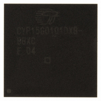
CYP15G0101DXB-BBXC Cypress Semiconductor Corp, CYP15G0101DXB-BBXC Datasheet - Page 12

CYP15G0101DXB-BBXC
Manufacturer Part Number
CYP15G0101DXB-BBXC
Description
IC TXRX HOTLINK 100-LBGA
Manufacturer
Cypress Semiconductor Corp
Series
HOTlink II™r
Type
Transceiverr
Specifications of CYP15G0101DXB-BBXC
Package / Case
100-LBGA
Protocol
Fibre Channel
Voltage - Supply
3.135 V ~ 3.465 V
Mounting Type
Surface Mount
Product
PHY
Data Rate
1500 MBd
Supply Voltage (max)
3.465 V
Supply Voltage (min)
3.135 V
Supply Current
0.5 A
Maximum Operating Temperature
+ 70 C
Minimum Operating Temperature
0 C
Mounting Style
SMD/SMT
Number Of Channels
1
Lead Free Status / RoHS Status
Lead free / RoHS Compliant
For Use With
CYP15G0101DX-EVAL - EVAL BRD FOR HOTLINK II
Number Of Drivers/receivers
-
Lead Free Status / Rohs Status
Lead free / RoHS Compliant
Other names
428-2920
CYP15G0101DXB-BBXC
CYP15G0101DXB-BBXC
Available stocks
Company
Part Number
Manufacturer
Quantity
Price
Company:
Part Number:
CYP15G0101DXB-BBXC
Manufacturer:
MURATA
Quantity:
260 000
Company:
Part Number:
CYP15G0101DXB-BBXC
Manufacturer:
CYPRESS
Quantity:
206
Company:
Part Number:
CYP15G0101DXB-BBXC
Manufacturer:
Cypress Semiconductor Corp
Quantity:
10 000
Part Number:
CYP15G0101DXB-BBXC
Manufacturer:
CYPRESS/赛普拉斯
Quantity:
20 000
CYP(V)(W)15G0101DXB HOTLink II
Operation
The CYP(V)(W)15G0101DXB is a highly configurable device
designed to support reliable transfer of large quantities of data
using high-speed serial links from a single source to one or more
destinations.
CYP(V)(W)15G0101DXB Transmit Data Path
Operating Modes
The transmit path of the CYP(V)(W)15G0101DXB supports a
single character-wide data path. This data path is used in
multiple operating modes as controlled by the TXMODE[1:0]
inputs.
Input Register
The bits in the input register support different assignments,
based on if the character is unencoded, encoded with two control
bits, or encoded with three control bits. These assignments are
shown in
Table 1. Input Register Bit Assignments
The input register captures a minimum of eight data bits and two
control bits on each input clock cycle. When the encoder is
bypassed, the TXCT[1:0] control bits are part of the pre-encoded
10-bit data character.
When the encoder is enabled (TXMODE[1] LOW), the
TXCT[1:0] bits are interpreted along with the TXD[7:0] character
to generate the specific 10-bit transmission character. When
TXMODE[0] HIGH, an additional special character select
(SCSEL) input is also captured and interpreted. This SCSEL
input is used to modify the encoding of the characters.
Document Number: 38-02031 Rev. *L
Notes
10. The TXOP input is also captured in the input register, but its interpretation is under the separate control of PARCTL.
11. One or more K28.5 characters may be added or lost from the data stream during this reset operation. When used with non-Cypress devices that require a complete
TXCT[1]
Signal Name
TXD[0]
16-character Word Sync Sequence for proper receive elasticity buffer alignment, it is recommend that the sequence be followed by a second Word Sync Sequence
to ensure proper operation.
TXCT[0]
SCSEL
TXD[1]
TXD[2]
TXD[3]
TXD[4]
TXD[6]
TXD[7]
TXD5]
Table
(LSB)
(MSB)
1.
Unencoded
Bypassed)
(Encoder
DIN[0]
DIN[1]
DIN[2]
DIN[3]
DIN[4]
DIN[5]
DIN[6]
DIN[7]
DIN[8]
DIN[9]
N/A
TXCT[0]
TXCT[1]
Control
Two-bit
TXD[0]
TXD[1]
TXD[2]
TXD[3]
TXD[4]
TXD[5]
TXD[6]
TXD[7]
(Encoder Enabled)
N/A
[10]
Encoded
Three-bit
TXCT[0]
TXCT[1]
Control
SCSEL
TXD[0]
TXD[1]
TXD[2]
TXD[3]
TXD[4]
TXD[5]
TXD[6]
TXD[7]
Phase-Align Buffer
Data from the input register is passed either to the encoder or to
the phase-align buffer. When the transmit path is operated
synchronous
TXRATE = LOW), the phase-align buffer is bypassed and data is
passed directly to the parity check and encoder block to reduce
latency.
When an input register clock with an uncontrolled phase
relationship to REFCLK is selected (TXCKSEL LOW) or if data
is captured on both edges of REFCLK (TXRATE = HIGH), the
phase-align buffer is enabled. This buffer is used to absorb clock
phase differences between the presently selected input clock
and the internal character clock.
Initialization of the phase-align buffer takes place when the
TXRST input is sampled LOW by two consecutive rising edges
of REFCLK. When TXRST is returned HIGH, the present input
clock phase relative to REFCLK is set. TXRST is an
asynchronous input, but is sampled internally to synchronize it to
the internal transmit path state machine.
Once set, the input clock is allowed to skew in time up to half a
character period in either direction relative to REFCLK; that
is 180°. This time shift allows the delay path of the character
clock (relative to REFLCK) to change due to operating voltage
and temperature, while not affecting the design operation.
If the phase offset, between the initialized location of the input
clock and REFCLK, exceeds the skew handling capabilities of
the phase-align buffer, an error is reported on the TXPER output.
This output indicates a continuous error until the phase-align
buffer is reset. While the error remains active, the transmitter
outputs a continuous C0.7 character to indicate to the remote
receiver that an error condition is present in the link.
In specific transmit modes, it is also possible to reset the
phase-align buffer with minimal disruption of the serial data
stream. When the transmit interface is configured for generation
of atomic Word Sync Sequences (TXMODE[1] = MID) and a
phase-align buffer error is present, the transmission of a Word
Sync Sequence will recenter the phase-align buffer and clear the
error condition.
Parity Support
In addition to the ten data and control bits that are captured at
the transmit input register, a TXOP input is also available. This
allows the CYP(V)(W)15G0101DXB to support ODD parity
checking. Parity checking is available for all operating modes
(including encoder bypass). The specific mode of parity checking
is controlled by the PARCTL input, and operates per
When PARCTL = MID (open) and the encoder is enabled
(TXMODE[1] LOW), only the TXD[7:0] data bits are checked
for ODD parity along with the TXOP bit. When PARCTL = HIGH
with the encoder enabled (or MID with the encoder bypassed),
the TXD[7:0] and TXCT[1:0] inputs are checked for ODD parity
along with the TXOP bit. When PARCTL = LOW, parity checking
is disabled.
[11]
to
REFCLK
CYW15G0101DXB
CYP15G0101DXB
CYV15G0101DXB
(TXCKSEL = LOW
Page 12 of 44
Table
2.
and
[+] Feedback


