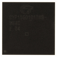
CYP15G0101DXB-BBXC Cypress Semiconductor Corp, CYP15G0101DXB-BBXC Datasheet - Page 16

CYP15G0101DXB-BBXC
Manufacturer Part Number
CYP15G0101DXB-BBXC
Description
IC TXRX HOTLINK 100-LBGA
Manufacturer
Cypress Semiconductor Corp
Series
HOTlink II™r
Type
Transceiverr
Specifications of CYP15G0101DXB-BBXC
Package / Case
100-LBGA
Protocol
Fibre Channel
Voltage - Supply
3.135 V ~ 3.465 V
Mounting Type
Surface Mount
Product
PHY
Data Rate
1500 MBd
Supply Voltage (max)
3.465 V
Supply Voltage (min)
3.135 V
Supply Current
0.5 A
Maximum Operating Temperature
+ 70 C
Minimum Operating Temperature
0 C
Mounting Style
SMD/SMT
Number Of Channels
1
Lead Free Status / RoHS Status
Lead free / RoHS Compliant
For Use With
CYP15G0101DX-EVAL - EVAL BRD FOR HOTLINK II
Number Of Drivers/receivers
-
Lead Free Status / Rohs Status
Lead free / RoHS Compliant
Other names
428-2920
CYP15G0101DXB-BBXC
CYP15G0101DXB-BBXC
Available stocks
Company
Part Number
Manufacturer
Quantity
Price
Company:
Part Number:
CYP15G0101DXB-BBXC
Manufacturer:
MURATA
Quantity:
260 000
Company:
Part Number:
CYP15G0101DXB-BBXC
Manufacturer:
CYPRESS
Quantity:
206
Company:
Part Number:
CYP15G0101DXB-BBXC
Manufacturer:
Cypress Semiconductor Corp
Quantity:
10 000
Part Number:
CYP15G0101DXB-BBXC
Manufacturer:
CYPRESS/赛普拉斯
Quantity:
20 000
Serial Output Drivers
The serial interface output drivers use high-performance
differential current mode logic (CML) to provide source-matched
drivers for the transmission lines. These serial drivers accept
data from the transmit shifter. These outputs have signal swings
equivalent to that of standard PECL drivers, and are capable of
driving AC-coupled optical modules or AC-coupled transmission
lines. To acheive OBSAI RP3 compliancy, the serial output
drivers must be AC-coupled to the transmission medium.
When configured for local loop-back (LPEN = HIGH), the
enabled serial drivers are configured to drive a static differential
logic-1.
Each serial driver can be enabled or disabled through the
BOE[1:0] inputs, as controlled by the OELE latch-enable signal.
When OELE = HIGH, the signals present on the BOE[1:0] inputs
are passed through the serial output enable latch to control the
serial driver. The BOE[1:0] input with OUT1 and OUT2driver
is listed in
Table 8. Output Enable, BIST, and Receive Channel Enable
Signal Map
When OELE = HIGH and BOE[x] = HIGH, the associated serial
driver is enabled to drive any attached transmission line. When
OELE = HIGH and BOE[x] = LOW, the associated driver is
disabled and internally configured for minimum power
dissipation. If both serial drivers for the channel are disabled, the
internal logic for the transmit channel is also configured for
lowest power operation. When OELE returns LOW, the values
present on the BOE[1:0] inputs are latched in the output enable
latch, and remain there until OELE returns HIGH to open the
latch again. A device reset (TRSTZ sampled LOW) clears this
latch and disables both serial drivers.
Note. When both serial output drivers are disabled and a driver
is re-enabled, the data on the serial drivers may not meet all
timing specifications for up to 200 µs.
Transmit PLL Clock Multiplier
The transmit PLL clock multiplier accepts a character-rate or
half-character-rate external clock at the REFCLK input, and
multiples that clock by 10 or 20 (as selected by TXRATE) to
generate a bit-rate clock for use by the transmit shifter. It also
provides a character-rate clock used by the transmit path.
This clock multiplier PLL can accept a REFCLK input between
19.5 MHz
CYW15G0101DXB), however, this clock range is limited by the
operating mode of the CYP(V)(W)15G0101DXB clock multiplier
(controlled by TXRATE) and by the level on the SPDSEL input.
Document Number: 38-02031 Rev. *L
Note
16. When REFCLK is configured for half-rate operation (TXRATE
BOE Input
REFCLK.
BOE[1]
BOE[0]
Table
and
8.
Controlled
150 MHz
(OELE)
Output
OUT2
OUT1
(19.5 MHz
(BISTLE)
Channel
Transmit
Receive
Enable
BIST
and
Receive PLL
Channel
154 MHz
Receive
Enable
(RXLE)
=
X
HIGH), this input is sampled (or the outputs change) relative to both the rising and falling edges of
for
When TXRATE=HIGH, configuring TXCKSEL = HIGH or MID is
an invalid mode of operation.
SPDSEL is a 3-level select
three operating ranges for the serial data outputs and inputs. The
operating serial signaling-rate and allowable range of REFCLK
frequencies are listed in
Table 9. Operating Speed Settings
The REFCLK input is a differential input with each input
internally biased to 1.4 V. If the REFCLK+ input is connected to
a TTL, LVTTL, or LVCMOS clock source, the input signal is
recognized when it passes through the internally biased
reference point.
When both the REFCLK+ and REFCLK inputs are connected,
the clock source must be a differential clock. This can be either
a differential LVPECL clock that is DC- or AC-coupled, or a
differential LVTTL or LVCMOS clock.
By connecting the REFCLK input to an external voltage source
or resistive voltage divider, it is possible to adjust the reference
point of the REFCLK+ input for alternate logic levels. When doing
so, it is necessary to ensure that the 0 V-differential crossing
point remains within the parametric range supported by the input.
CYP(V)(W)15G0101DXB Receive Data Path
Serial Line Receivers
Two differential line receivers, IN1and IN2, are available for
accepting serial data streams. The active serial line receiver is
selected using the INSEL input. Both serial line receivers have
differential inputs, and can accommodate wire interconnect and
filtering losses or transmission line attenuation greater than
16 dB. For normal operation, these inputs should receive a
signal of at least V
differential. Each line receiver can be DC- or AC-coupled to
+3.3 V powered fiber-optic interface modules (any ECL/PECL
logic family, not limited to 100 K PECL) or AC-coupled to
+5 V-powered optical modules. The common-mode tolerance of
the receivers accommodates a wide range of signal termination
voltages. Each receiver provides internal DC-restoration, to the
center of the receiver’s common mode range, for AC-coupled
signals.
MID (Open)
SPDSEL
HIGH
LOW
TXRATE
DIFFS
1
0
1
0
1
0
Table
> 100 mV, or 200-mV peak-to-peak
[16]
Frequency
Reserved
REFCLK
(ternary) input that selects one of
9.
19.5–40
80–150
20–40
40–80
40–75
(MHz)
CYW15G0101DXB
CYP15G0101DXB
CYV15G0101DXB
CYW15G0101DXB)
Signaling Rate
(800–1540 for
800–1500
(MBaud)
195–400
400–800
Page 16 of 44
[+] Feedback


