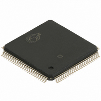
CY7C9689A-AXC Cypress Semiconductor Corp, CY7C9689A-AXC Datasheet - Page 43

CY7C9689A-AXC
Manufacturer Part Number
CY7C9689A-AXC
Description
IC TXRX HOTLINK 100LQFP
Manufacturer
Cypress Semiconductor Corp
Series
CY7Cr
Type
Transceiverr
Datasheet
1.CY7C9689A-AXC.pdf
(51 pages)
Specifications of CY7C9689A-AXC
Package / Case
100-LQFP
Voltage - Supply
4.5 V ~ 5.5 V
Mounting Type
Surface Mount
Product
PHY
Interface Type
Parallel
Supply Voltage (max)
6.5 V
Supply Voltage (min)
2 V
Supply Current
250 mA
Maximum Operating Temperature
+ 70 C
Minimum Operating Temperature
0 C
Mounting Style
SMD/SMT
Number Of Channels
2
Ic Interface Type
Parallel, Serial
Supply Voltage Range
4.5V To 5.5V
Operating Temperature Range
0°C To +70°C
Digital Ic Case Style
TQFP
No. Of Pins
100
Msl
MSL 3 - 168 Hours
No. Of Receivers
2
Rohs Compliant
Yes
Frequency Max
50MHz
Lead Free Status / RoHS Status
Lead free / RoHS Compliant
Number Of Drivers/receivers
-
Protocol
-
Lead Free Status / Rohs Status
Lead free / RoHS Compliant
Available stocks
Company
Part Number
Manufacturer
Quantity
Price
Company:
Part Number:
CY7C9689A-AXC
Manufacturer:
ALTERA
Quantity:
112
Company:
Part Number:
CY7C9689A-AXC
Manufacturer:
CY
Quantity:
86
Company:
Part Number:
CY7C9689A-AXC
Manufacturer:
CYPRESS
Quantity:
273
Company:
Part Number:
CY7C9689A-AXC
Manufacturer:
Cypress Semiconductor Corp
Quantity:
10 000
Part Number:
CY7C9689A-AXC
Manufacturer:
CYPRESS/赛普拉斯
Quantity:
20 000
Document #: 38-02020 Rev. *E
The selection state of the Receive FIFO is entered when an
Rx_Match condition is present, and RXEN transitions from
HIGH to LOW. Once selected, the Receive FIFO remains
selected until RXEN is sampled HIGH by the rising edge of
Synchronous With UTOPIA Timing and Control
(Receive FIFO Bypassed)
When the Receive FIFO is bypassed (FIFOBYP is LOW), the
CY7C9689A must still be selected to enable the output drivers
for the RXDATA bus. With the Receive FIFO bypassed,
RXCLK becomes a synchronous output clock operating at the
character rate.
When CE is sampled LOW and RXRST is sampled HIGH by
the rising edge of RXCLK output, an Rx_Match condition is
generated. This Rx_Match condition continues until CE is
sampled HIGH or RXRST is sampled LOW at the rising edge
of RXCLK.
When an Rx_Match (or Rx_RstMatch) condition is present,
the RXEMPTY and RXFULL output drivers are enabled. With
TXDATA/TXCMD
TXDATA/TXCMD
(Shared Bus Timing)
(Cascade Timing)
Tx_Selected
Tx_Match
REFCLK
TXFULL
TXRST
TXEN
CE
[46]
[46]
Figure 9. Transmit Selection with Transmit FIFO Bypassed
Note 47
Note 47
Not Full
RXCLK input. The selected state initiates a read cycle from the
Receive FIFO and enables the Receive FIFO data onto the
RXDATA bus. This receive interface selection process is
shown in
the Receive FIFO bypassed, these flags normally indicate a
non-empty condition but may indicate empty if a JK or LM
SYNC character is present in the output register and the
receiver discard policy is non-0. When an Rx_Match (or
Rx_RstMatch) condition is not present, these same drivers are
disabled (High-Z).
The selection state of the Receive Output Register is entered
when an Rx_Match condition is present, and RXEN transitions
from HIGH to LOW. Once selected, the Receive Output
Register remains selected until RXEN is sampled HIGH by the
rising edge of RXCLK output. In the selected state, the output
drivers for the RXDATA outputs are enabled, and new data is
presented to the RXDATA bus on every clock cycle
Not Full
D1
Figure 10
D2
D1
D3
D2
D3
CY7C9689A
Page 43 of 51
[+] Feedback


