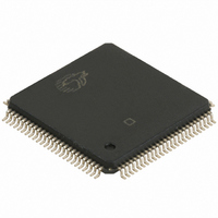
CY7C9689A-AXC Cypress Semiconductor Corp, CY7C9689A-AXC Datasheet - Page 6

CY7C9689A-AXC
Manufacturer Part Number
CY7C9689A-AXC
Description
IC TXRX HOTLINK 100LQFP
Manufacturer
Cypress Semiconductor Corp
Series
CY7Cr
Type
Transceiverr
Datasheet
1.CY7C9689A-AXC.pdf
(51 pages)
Specifications of CY7C9689A-AXC
Package / Case
100-LQFP
Voltage - Supply
4.5 V ~ 5.5 V
Mounting Type
Surface Mount
Product
PHY
Interface Type
Parallel
Supply Voltage (max)
6.5 V
Supply Voltage (min)
2 V
Supply Current
250 mA
Maximum Operating Temperature
+ 70 C
Minimum Operating Temperature
0 C
Mounting Style
SMD/SMT
Number Of Channels
2
Ic Interface Type
Parallel, Serial
Supply Voltage Range
4.5V To 5.5V
Operating Temperature Range
0°C To +70°C
Digital Ic Case Style
TQFP
No. Of Pins
100
Msl
MSL 3 - 168 Hours
No. Of Receivers
2
Rohs Compliant
Yes
Frequency Max
50MHz
Lead Free Status / RoHS Status
Lead free / RoHS Compliant
Number Of Drivers/receivers
-
Protocol
-
Lead Free Status / Rohs Status
Lead free / RoHS Compliant
Available stocks
Company
Part Number
Manufacturer
Quantity
Price
Company:
Part Number:
CY7C9689A-AXC
Manufacturer:
ALTERA
Quantity:
112
Company:
Part Number:
CY7C9689A-AXC
Manufacturer:
CY
Quantity:
86
Company:
Part Number:
CY7C9689A-AXC
Manufacturer:
CYPRESS
Quantity:
273
Company:
Part Number:
CY7C9689A-AXC
Manufacturer:
Cypress Semiconductor Corp
Quantity:
10 000
Part Number:
CY7C9689A-AXC
Manufacturer:
CYPRESS/赛普拉斯
Quantity:
20 000
Document #: 38-02020 Rev. *E
Pin Descriptions
70
60
8
41, 43,
45, 47,
48, 53,
59,61
Receive Path Signals
Pin
TXHALF
TXEMPTY
RXCLK
RXDATA[7:0]
Name
(continued)
Three-state TTL
output, changes
following TXCLK↑
Three-state TTL
output, changes
following TXCLK↑ or
REFCLK↑
Bidirectional TTL clock
Internal Pull-up
Three-state TTL
output, changes
following RXCLK↑
I/O Characteristics
Transmit FIFO Half-full Status Flag.
When the Transmit FIFO is enabled (FIFOBYP is HIGH and CE is LOW)
TXHALF is asserted when the HOTLink Transmit FIFO is half full (128
characters is half full). If a Transmit FIFO reset has been initiated (TXRST was
sampled asserted for a minimum of seven TXCLK cycles), TXHALF is asserted
to enforce the full/unavailable status of the Transmit FIFO during reset.
When the Transmit FIFO is bypassed (FIFOBYP is LOW), TXHALF remains
deasserted, having no logical function.
TXHALF is forced to the High-Z state only during a “full-chip” reset (i.e., while
RESET is LOW).
Transmit FIFO Empty Status Flag.
When the Transmit FIFO is enabled (FIFOBYP is HIGH and CE is LOW),
TXEMPTY is asserted when the HOTLink Transmit FIFO has no data to forward
to the encoder. If a Transmit FIFO reset has been initiated (TXRST was sampled
asserted for a minimum of seven TXCLK cycles), TXEMPTY is deasserted and
remains deasserted until the Transmit FIFO reset operation is complete.
When the Transmit FIFO is bypassed (FIFOBYP is LOW), TXEMPTY is
asserted to indicate that the transmitter can accept data. TXEMPTY is also used
as a BIST progress indicator when TXBISTEN is asserted.
When TXBISTEN is asserted LOW, TXEMPTY becomes the transmit BIST-loop
counter indicator (regardless of the logic state of FIFOBYP). In this mode
TXEMPTY is asserted for one TXCLK or REFCLK period at the end of each
transmitted BIST sequence.
Note: During BIST operations, when the Transmit FIFO is enabled (FIFOBYP
is HIGH), it is necessary to keep TXCLK operating, even though no data is
loaded into the Transmit FIFO and TXEN is never asserted, to allow the
TXEMPTY flag to respond to the BIST state changes.
The asserted state of this output (HIGH or LOW) is determined by the state of
the EXTFIFO input. When EXTFIFO is LOW, TXEMPTY is active LOW. When
EXTFIFO is HIGH, TXEMPTY is active HIGH.
If CE is sampled asserted (LOW), TXEMPTY is driven to an active state. If CE
is sampled deasserted (HIGH), TXEMPTY is placed into a High-Z state.
Receive Clock.
When the Receive FIFO is enabled (FIFOBYP is HIGH), this clock is the
Receive interface input clock and is used to control Receive FIFO read and
reset, operations. When the Receive FIFO is bypassed (FIFOBYP is LOW), this
clock becomes the recovered Receive PLL character clock output which runs
continuously at the character rate.
Parallel Receive DATA Outputs.
When the decoder is enabled (ENCBYP is HIGH), the low-order eight bits of
the decoded DATA character are presented on the RXDATA[7:0] outputs.
COMMAND characters, when they are received, do not disturb these outputs.
When the decoder is bypassed, the low order eight bits of the non-decoded
character are presented on the RXDATA[7:0] outputs.
When the Receive FIFO is disabled (FIFOBYP is LOW), these outputs change
on the rising edge of the RXCLK output. When the Receive FIFO is enabled
(FIFOBYP is HIGH), these outputs change on the rising edge of RXCLK input.
RXEN is the three-state control for RXDATA[7:0].
Signal Description
CY7C9689A
Page 6 of 51
[+] Feedback


