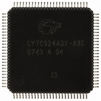
CY7C924ADX-AXC Cypress Semiconductor Corp, CY7C924ADX-AXC Datasheet - Page 43

CY7C924ADX-AXC
Manufacturer Part Number
CY7C924ADX-AXC
Description
IC TXRX HOTLINK 100LQFP
Manufacturer
Cypress Semiconductor Corp
Series
HOTlink™r
Type
Transceiverr
Specifications of CY7C924ADX-AXC
Package / Case
100-LQFP
Protocol
Fibre Channel
Voltage - Supply
4.5 V ~ 5.5 V
Mounting Type
Surface Mount
Product
Framer
Number Of Transceivers
1
Data Rate
622 Mbps
Supply Voltage (max)
5.5 V
Supply Voltage (min)
4.5 V
Supply Current (max)
250 mA
Maximum Operating Temperature
+ 70 C
Minimum Operating Temperature
0 C
Mounting Style
SMD/SMT
Operating Supply Voltage (typ)
5V
Screening Level
Commercial
Pin Count
100
Mounting
Surface Mount
Package Type
TQFP
Operating Supply Voltage (min)
4.5V
Operating Supply Voltage (max)
5.5V
Operating Temperature (min)
0C
Operating Temperature (max)
70C
Ic Interface Type
Parallel, Serial
Supply Voltage Range
4.5V To 5.5V
Operating Temperature Range
0°C To +70°C
Digital Ic Case Style
TQFP
No. Of Pins
100
No. Of Receivers
2
Frequency Max
50MHz
Rohs Compliant
Yes
Termination Type
SMD
Filter Terminals
SMD
Driver Case Style
TQFP
Lead Free Status / RoHS Status
Lead free / RoHS Compliant
Number Of Drivers/receivers
-
Lead Free Status / Rohs Status
Compliant
Other names
428-2918
CY7C924ADX-AXC
CY7C924ADX-AXC
Available stocks
Company
Part Number
Manufacturer
Quantity
Price
Company:
Part Number:
CY7C924ADX-AXC
Manufacturer:
CY
Quantity:
6
Company:
Part Number:
CY7C924ADX-AXC
Manufacturer:
CYPRESS
Quantity:
455
Company:
Part Number:
CY7C924ADX-AXC
Manufacturer:
Cypress Semiconductor Corp
Quantity:
10 000
The Cascade timing model is a modification of the UTOPIA
configuration that changes the flags and FIFO read/write
enables to active HIGH. This model is present primarily to allow
depth expansion of the internal FIFO by direct coupling to
external CY7C42x5 synchronous FIFOs. To allow this direct
coupling, the FIFO flag active levels and cycle-to-cycle timing
between the transmit enable (TXEN*) and data latching are
modified to ensure correct data transfer.
These four configurations of bus operation and timing/control
can all be used with or without external FIFOs. Depending on the
specific mode selected, the amount of external hardware
necessary to properly couple the CY7C924ADX to state
machines or external FIFOs is minimal in all cases, and may be
zero if the proper configuration is selected.
UTOPIA Interface Background
The UTOPIA interface is defined by the ATM Forum as the bus
interface between the ATM and PHY layer devices of an ATM
system. This interface is defined as 8 or 16 bits wide, with the
latter reserved mainly for high-speed physical interfaces (PHYs)
such as 622 Mbps OC-12. Due to the limited speed range of the
CY7C924, only the 8-bit interface is implemented.
UTOPIA-1 was the original UTOPIA specification (created in
1993) which covers transport of:
■
■
■
■
■
The UTOPIA-1 interface has a maximum clock rate of 25 MHz.
All AC-timing and pin descriptions are covered in the UTOPIA-1
Specification, Version 2.01.
UTOPIA-2 was created as an addendum to the UTOPIA-1 speci-
fication. In this revision, the parallel interface was extended to
both 33 MHz and 50 MHz to accommodate PCI bus architec-
tures in ATM designs. A method of addressing was added to
allow multiple devices (PHYs) to share a common host bus. Also,
a description of a management interface was added (not
supported by this device).
The CY7C924ADX contains all pins necessary to support the
UTOPIA-1 and, through use of an external address decoder, can
emulate the multi-PHY capability of a UTOPIA-2 interface. The
maximum bus speed supports the full 50 MHz I/O rate for
emerging high-performance systems.
UTOPIA Address Match and Selection
All actions on a UTOPIA-2 interface are controlled by the
Address Match and selection states of the interface. These
states control the read and write access to the Receive and
Transmit FIFOs, access to the FIFO status flags, reset of the
Transmit and Receive FIFOs, and read and write access to the
Serial Address Register. The CY7C924ADX supports the
concept of an “address match” through a single Address Match
(AM*) input.
Document #: 38-02008 Rev. *G
155.52 Mbps (scrambled SONET/OC-3)
155.52 Mbps (8B/10B block coded at 194.4 MBaud)
100 Mbps (4B/5B encoded TAXI)
44.736 Mbps (DS-3/T3)
51.84 Mbps (OC-1)
Address Match and FIFO Flag Access
The CY7C924ADX makes use of a single active-LOW Address
Match (AM*) to generate address-match conditions. When this
input is LOW it is equivalent to an ATM address compare on both
the TXADDR and RXADDR buses. This allows multiple
CY7C924ADX devices to share a common bus, with device
output three-state controls being managed by either an address
match condition (AM* sampled LOW), or by a selection state.
The Transmit and Receive FIFO flag empty and FIFO full output
drivers are enabled in any TXCLK, REFCLK, or RXCLK cycle
following AM* being sampled asserted (LOW) by the rising edge
of the respective clock. The AM* input is sampled separately by
the clocks for the transmit and receive interfaces, which allows
these clocks to operate at different clock rates. An example of
both Transmit and Receive FIFO flag access is shown in
Figure
Figure 9. FIFO Flag Driver Enables
When the Transmit FIFO is enabled (FIFOBYP* is HIGH) and
AM* is sampled LOW by the rising edge of TXCLK, the output
drivers for the TXFULL* and TXEMPTY* FIFO flags are enabled.
When AM* is sampled HIGH by the rising edge of TXCLK, these
same output drivers are disabled.
When the Transmit FIFO is bypassed (FIFOBYP* is LOW and
not in byte-packed mode) and AM* is sampled LOW by the rising
edge of REFCLK, the output drivers for the TXFULL* and
TXEMPTY* FIFO flags are enabled. When AM* is sampled HIGH
by the rising edge of REFCLK, the FIFO flag output drivers are
disabled.
When AM* is sampled LOW by the rising edge of RXCLK (input
or output), the output drivers for the RXFULL* and RXEMPTY*
FIFO flags are enabled. When AM* is sampled HIGH by the
rising edge of RXCLK, the FIFO flag output drivers are disabled.
RXEMPTY*
TXFULL*
RXCLK
TXCLK
9.
AM*
AM*
Transmit Port Addressing
Receive Port Addressing
Valid
Valid
CY7C924ADX
Page 43 of 62


