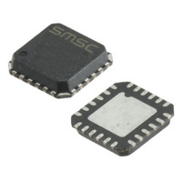
LAN8700IC-AEZG SMSC, LAN8700IC-AEZG Datasheet - Page 14

LAN8700IC-AEZG
Manufacturer Part Number
LAN8700IC-AEZG
Description
TXRX ETHERNET 10/100 IND 36-QFN
Manufacturer
SMSC
Type
Transceiverr
Datasheet
1.LAN8700C-AEZG.pdf
(80 pages)
Specifications of LAN8700IC-AEZG
Protocol
MII, RMII
Voltage - Supply
3 V ~ 3.6 V
Mounting Type
Surface Mount
Package / Case
36-QFN
Supply Voltage Range
3V To 3.6V
Digital Ic Case Style
QFN
No. Of Pins
36
Operating Temperature Range
-40°C To +85°C
Control Interface
MII, RMII
Data Rate Max
100Mbps
Rohs Compliant
Yes
Lead Free Status / RoHS Status
Lead free / RoHS Compliant
Number Of Drivers/receivers
-
Other names
638-1047-6
Available stocks
Company
Part Number
Manufacturer
Quantity
Price
Company:
Part Number:
LAN8700IC-AEZG
Manufacturer:
SANKEN
Quantity:
300
Company:
Part Number:
LAN8700IC-AEZG
Manufacturer:
Standard
Quantity:
34 317
Part Number:
LAN8700IC-AEZG
Manufacturer:
SMSC
Quantity:
20 000
Part Number:
LAN8700IC-AEZG-C3
Manufacturer:
SMSC
Quantity:
20 000
Part Number:
LAN8700IC-AEZG-TR
Manufacturer:
MICROCHIP/微芯
Quantity:
20 000
Revision 2.2 (12-04-09)
SIGNAL NAME
SIGNAL NAME
SPEED100/
RX_CLK/
REGOFF
CRS_DV
PHYAD4
PHYAD0
RX_ER/
RX_DV
RXD4/
RMII/
CRS/
COL/
TYPE
TYPE
IOPD
IOPD
IOPU
IOPU
Table 3.1 MII Signals (continued)
OPD
±15kV ESD Protected MII/RMII 10/100 Ethernet Transceiver with HP Auto-MDIX Support and flexPWR
O
Table 3.2 LED Signals
DATASHEET
Receive Error: Asserted to indicate that an error was detected
somewhere in the frame presently being transferred from the
PHY.
MII Receive Data 4: In Symbol Interface (5B Decoding) mode,
this signal is the MII Receive Data 4 signal, the MSB of the
received 5-bit symbol code-group. Unless configured in this
mode, the pin functions as RX_ER.
Note:
Receive Data Valid: Indicates that recovered and decoded data
nibbles are being presented on RXD[3:0].
Note:
Receive Clock: In MII mode, this pin is the receive clock output.
25MHz in 100Base-TX mode. 2.5MHz in 10Base-T mode.
Note:
Regulator Off: This pin pulled up to configure the internal 1.8V
regulator off. As described in
during the power-on sequence to determine if the internal
regulator should turn on. When the regulator is disabled, external
1.8V must be supplied to VDD_CORE, and the voltage at VDD33
must be at least 2.64V before voltage is applied to VDD_CORE.
MII Mode Collision Detect: Asserted to indicate detection of
collision condition.
RMII – MII/RMII mode selection is latched on the rising edge of
the internal reset (nreset) based on the following strapping:
RMII Mode CRS_DV (Carrier Sense/Receive Data Valid)
Asserted to indicate when the receive medium is non-idle. When
a 10BT packet is received, CRS_DV is asserted, but RXD[1:0] is
held low until the SFD byte (10101011) is received. In 10BT, half-
duplex mode, transmitted data is not looped back onto the
receive data pins, per the RMII standard.
Carrier Sense: Indicates detection of carrier.
Note:
LED1 – SPEED100 indication. Active indicates that the selected
speed is 100Mbps. Inactive indicates that the selected speed is
10Mbps.
Note:
Float this pin for MII mode or pull-high with an external resistor
to VDDIO (see
Resistors,” on page
See
more details.
Section 4.6.3, "MII vs. RMII Configuration," on page 26
14
This pin has an internal pull-down resistor, and must not
be high during reset. The RX_ER signal is optional in
RMII Mode.
This pin has an internal pull-down resistor, and must not
be high during reset. This signal is not used in RMII
Mode.
This signal is not used in RMII Mode.
This signal is mux’d with PHYAD4
This signal is mux’d with PHYAD0
Table 4.3, “Boot Strapping Configuration
32) to set the device in RMII mode.
DESCRIPTION
DESCRIPTION
Section
4.9, this pin is sampled
SMSC LAN8700/LAN8700i
®
Technology in a Small Footprint
Datasheet
for


