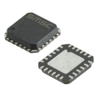
LAN8700IC-AEZG SMSC, LAN8700IC-AEZG Datasheet - Page 23

LAN8700IC-AEZG
Manufacturer Part Number
LAN8700IC-AEZG
Description
TXRX ETHERNET 10/100 IND 36-QFN
Manufacturer
SMSC
Type
Transceiverr
Datasheet
1.LAN8700C-AEZG.pdf
(80 pages)
Specifications of LAN8700IC-AEZG
Protocol
MII, RMII
Voltage - Supply
3 V ~ 3.6 V
Mounting Type
Surface Mount
Package / Case
36-QFN
Supply Voltage Range
3V To 3.6V
Digital Ic Case Style
QFN
No. Of Pins
36
Operating Temperature Range
-40°C To +85°C
Control Interface
MII, RMII
Data Rate Max
100Mbps
Rohs Compliant
Yes
Lead Free Status / RoHS Status
Lead free / RoHS Compliant
Number Of Drivers/receivers
-
Other names
638-1047-6
Available stocks
Company
Part Number
Manufacturer
Quantity
Price
Company:
Part Number:
LAN8700IC-AEZG
Manufacturer:
SANKEN
Quantity:
300
Company:
Part Number:
LAN8700IC-AEZG
Manufacturer:
Standard
Quantity:
34 317
Part Number:
LAN8700IC-AEZG
Manufacturer:
SMSC
Quantity:
20 000
Part Number:
LAN8700IC-AEZG-C3
Manufacturer:
SMSC
Quantity:
20 000
Part Number:
LAN8700IC-AEZG-TR
Manufacturer:
MICROCHIP/微芯
Quantity:
20 000
±15kV ESD Protected MII/RMII 10/100 Ethernet Transceiver with HP Auto-MDIX Support and flexPWR
Datasheet
SMSC LAN8700/LAN8700i
4.3.8
4.3.9
4.4
4.4.1
Receiver Errors
During a frame, unexpected code-groups are considered receive errors. Expected code groups are the
DATA set (0 through F), and the /T/R/ (ESD) symbol pair. When a receive error occurs, the RX_ER
signal is asserted and arbitrary data is driven onto the RXD[3:0] lines. Should an error be detected
during the time that the /J/K/ delimiter is being decoded (bad SSD error), RX_ER is asserted true and
the value ‘1110’ is driven onto the RXD[3:0] lines. Note that the Valid Data signal is not yet asserted
when the bad SSD error occurs.
100M Receive Data Across the MII/RMII Interface
In MII mode, the 4-bit data nibbles are sent to the MII block. These data nibbles are clocked to the
controller at a rate of 25MHz. The controller samples the data on the rising edge of RX_CLK. To ensure
that the setup and hold requirements are met, the nibbles are clocked out of the PHY on the falling
edge of RX_CLK. RX_CLK is the 25MHz output clock for the MII bus. It is recovered from the received
data to clock the RXD bus. If there is no received signal, it is derived from the system reference clock
(CLKIN).
When tracking the received data, RX_CLK has a maximum jitter of 0.8ns (provided that the jitter of the
input clock, CLKIN, is below 100ps).
In RMII mode, the 2-bit data nibbles are sent to the RMII block. These data nibbles are clocked to the
controller at a rate of 50MHz. The controller samples the data on the rising edge of CLKIN/XTAL1
(REF_CLK). To ensure that the setup and hold requirements are met, the nibbles are clocked out of
the PHY on the falling edge of CLKIN/XTAL1 (REF_CLK).
Data to be transmitted comes from the MAC layer controller. The 10Base-T transmitter receives 4-bit
nibbles from the MII at a rate of 2.5MHz and converts them to a 10Mbps serial data stream. The data
stream is then Manchester-encoded and sent to the analog transmitter, which drives a signal onto the
twisted pair via the external magnetics.
The 10M transmitter uses the following blocks:
10M Transmit Data Across the MII/RMII Interface
The MAC controller drives the transmit data onto the TXD BUS. For MII, when the controller has driven
TX_EN high to indicate valid data, the data is latched by the MII block on the rising edge of TX_CLK.
The data is in the form of 4-bit wide 2.5MHz data.
In order to comply with legacy 10Base-T MAC/Controllers, in Half-duplex mode the PHY loops back
the transmitted data, on the receive path. This does not confuse the MAC/Controller since the COL
signal is not asserted during this time. The PHY also supports the SQE (Heartbeat) signal. See
5.4.2, "Collision Detect," on page
For RMII, TXD[1:0] shall transition synchronously with respect to REF_CLK. When TX_EN is asserted,
TXD[1:0] are accepted for transmission by the LAN8700/LAN8700i. TXD[1:0] shall be “00” to indicate
idle when TX_EN is deasserted. Values of TXD[1:0] other than “00” when TX_EN is deasserted are
reserved for out-of-band signalling (to be defined). Values other than “00” on TXD[1:0] while TX_EN is
deasserted shall be ignored by the LAN8700/LAN8700i.TXD[1:0] shall provide valid data for each
REF_CLK period while TX_EN is asserted.
10Base-T Transmit
MII (digital)
TX 10M (digital)
10M Transmitter (analog)
10M PLL (analog)
50, for more details.
DATASHEET
®
23
Technology in a Small Footprint
Revision 2.2 (12-04-09)
Section


