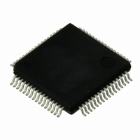
VSC8601XKN Vitesse Semiconductor Corp, VSC8601XKN Datasheet - Page 85

VSC8601XKN
Manufacturer Part Number
VSC8601XKN
Description
IC PHY 10/100/1000 64-EP-LQFP
Manufacturer
Vitesse Semiconductor Corp
Type
PHY Transceiverr
Specifications of VSC8601XKN
Number Of Drivers/receivers
1/1
Protocol
Gigabit Ethernet
Voltage - Supply
2.5V, 3.3V
Mounting Type
Surface Mount
Package / Case
64-LQFP Exposed Pad, 64-eLQFP, 64-HLQFP
Case
TQFP
Dc
06+
Lead Free Status / RoHS Status
Lead free / RoHS Compliant
Other names
907-1028
Available stocks
Company
Part Number
Manufacturer
Quantity
Price
Company:
Part Number:
VSC8601XKN
Manufacturer:
KYOCERA/AVX
Quantity:
20 000
Company:
Part Number:
VSC8601XKN
Manufacturer:
VITESSE
Quantity:
1 235
Company:
Part Number:
VSC8601XKN
Manufacturer:
Vitesse Semiconductor Corporation
Quantity:
10 000
Part Number:
VSC8601XKN
Manufacturer:
VITESSE
Quantity:
20 000
6.2
Table 78.
6.2.1
Table 79.
Revision 4.1
September 2009
Pins by Function
This section contains the functional pin descriptions for the VSC8601 device. The
following table contains notations for definitions of the various pin types.
Pin Type Symbols
Twisted Pair Interface
The following table lists the device pins associated with the device two-wire, twisted
pair interface.
Twisted Pair Interface Pins
Pin
53
54
55
56
58
59
60
61
Symbol
O
I
I
A
A
I
PD
PU
O
CRYST
PU5V
I/O
OD
I
I
OS
NC
BIAS
DIFF
I
O
PU
PD
I
ZC
A
/O
/O
Name
TXVPA
TXVNA
TXVPB
TXVNB
TXVPC
TXVNC
TXVPD
TXVND
Pin Type
Input
Input and Output
Input with pull-up
Input with pull-down
Bidirectional with
pull-down
Bidirectional with
pull-up
Output
Impedance controlled
output
Open drain
Open source
Analog differential
Analog bias
Analog input
Input with pull-up
Crystal output
No connect
Type
A
A
A
A
A
A
A
A
DIFF
DIFF
DIFF
DIFF
DIFF
DIFF
DIFF
DIFF
Description
TX/RX channel A positive signal
TX/RX channel A negative signal
TX/RX channel B positive signal
TX/RX channel B negative signal
TX/RX channel C positive signal
TX/RX channel C negative signal
TX/RX channel D positive signal
TX/RX channel D negative signal
Description
Input with no on-chip pull-up or pull-down resistor.
Input and output signal with no on-chip pull-up or
pull-down resistor.
Input with on-chip 100 kΩ pull-up resistor to VDDIO.
Input with on-chip 100 kΩ pull-down resistor to VSS.
Input and output signal with on-chip 100 kΩ pull-down
resistor to VSS.
Input and output signal with on-chip 100 kΩ pull-up
resistor to VDDIO or VDD33.
Output signal.
Integrated (on-chip) source series terminated, output
signal.
Open drain output.
Open source output.
Analog differential signal pair for twisted pair interface.
Analog bias pin.
Analog Input for sensing variable voltage levels.
Input with on-chip 100 kΩ pull-up resistor to VDD33.
These pins are 5 V tolerant.
Crystal clock output pin. If not used, leave unconnected.
No connect pins must be left floating.
VSC8601 Datasheet
Pin Descriptions
Page 85


