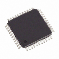
DS2148T+ Maxim Integrated Products, DS2148T+ Datasheet - Page 23

DS2148T+
Manufacturer Part Number
DS2148T+
Description
IC LIU E1/T1/J1 5V 44-TQFP
Manufacturer
Maxim Integrated Products
Type
Line Interface Units (LIUs)r
Specifications of DS2148T+
Number Of Drivers/receivers
1/1
Protocol
T1/E1/J1
Voltage - Supply
4.75 V ~ 5.25 V
Mounting Type
Surface Mount
Package / Case
44-TQFP, 44-VQFP
Lead Free Status / RoHS Status
Lead free / RoHS Compliant
3 HARDWARE MODE
In hardware mode (BIS1 = 1, BIS0 = 1), pins 1-19, 23, 25, 31, and 44 are redefined to be used for
initializing the DS2148. BPCLK (pin 31) defaults to a 16.384MHz output when in hardware mode. The
RCL/LOTC (pin 25) is designated to RCL when in hardware mode. JABDS (CCR4.2) defaults to logic 0.
The RHBE (CCR2.3) and THBE (CCR2.2) control bits are combined and controlled by HBE at pin 11
while the RSCLKE (CCR5.3) and TSCLKE (CCR5.2) bits are combined and controlled by SCLKE at
pin 4. TCES (CCR2.1) and RCES (CCR2.0) are combined and controlled by CES at pin 12. The
transmitter functions are combined and controlled by TX1 (pin 15) and TX0 (pin 14). LOOP1 (pin 17)
and LOOP0 (pin 16) control the loopback functions. All other control bits default to the logic 0 setting.
3.1 Register Map
Table 3-1. Register Map
NOTES:
1) Register addresses 16h to 1Fh do not exist.
2) In the Serial Port Mode, the LSB is on the right hand side.
3) In the Serial Port Mode, data is read and written LSB first.
4) In the Serial Port Mode, the A bit (the LSB) determines whether the access is a read (A = 1) or a write
5)
RDNCD1
RDNCD2
RUPCD1
RUPCD2
NAME
TEST1
TEST2
TEST3
CCR1
CCR2
CCR3
CCR4
CCR5
CCR6
TCD1
TCD2
ECR1
ECR2
IBCC
RIR1
RIR2
(A = 0).
In the Serial Port Mode, the B bit (the MSB) determines whether the access is a burst access (B = 1) or a single
register access (B = 0).
IMR
SR
–
Common Control Register 1
Common Control Register 2
Common Control Register 3
Common Control Register 4
Common Control Register 5
Common Control Register 6
Status Register
Interrupt Mask Register
Receive Information Register 1
Receive Information Register 2
In-Band Code Control Register
Transmit Code Definition Register 1
Transmit Code Definition Register 2
Receive Up Code Definition Register 1
Receive Up Code Definition Register 2
Receive Down Code Definition Register 1
Receive Down Code Definition Register 2
Error Count Register 1
Error Count Register 2
Test 1
Test 2
Test 3
REGISTER NAME
–
23 of 73
R/W
R/W
R/W
R/W
R/W
R/W
R/W
R/W
R/W
R/W
R/W
R/W
R/W
R/W
R/W
R/W
R/W
R/W
R
R
R
R
R
–
PORT MODE
PARALLEL
Note 1
0Ah
0Bh
0Ch
0Dh
0Eh
0Fh
00h
01h
02h
03h
04h
05h
06h
07h
08h
09h
10h
11h
12h
13h
14h
15h
SERIAL PORT
(msb)
(Notes 2–5)
B000 000A
B000 001A
B000 010A
B000 011A
B000 100A
B000 101A
B000 110A
B000 111A
B001 000A
B001 001A
B001 010A
B001 011A
B001 100A
B001 101A
B001 110A
B001 111A
B010 000A
B010 001A
B010 010A
B010 011A
B010 100A
B010 101A
MODE
–
(lsb)


