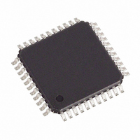
DS2148T+ Maxim Integrated Products, DS2148T+ Datasheet - Page 59

DS2148T+
Manufacturer Part Number
DS2148T+
Description
IC LIU E1/T1/J1 5V 44-TQFP
Manufacturer
Maxim Integrated Products
Type
Line Interface Units (LIUs)r
Specifications of DS2148T+
Number Of Drivers/receivers
1/1
Protocol
T1/E1/J1
Voltage - Supply
4.75 V ~ 5.25 V
Mounting Type
Surface Mount
Package / Case
44-TQFP, 44-VQFP
Lead Free Status / RoHS Status
Lead free / RoHS Compliant
9 DC CHARACTERISTICS
ABSOLUTE MAXIMUM RATINGS*
Voltage Range on Any Pin Relative to Ground……………………………………………..-1.0V to +6.0V
Operating Temperature Range for DS2148TN……………………………………………..-40°C to +85°C
Storage Temperature Range……………………………………………………………….-55°C to +125°C
Soldering Temperature………………………………………….See IPC/JEDEC J-STD-020 Specification
* This is a stress rating only and functional operation of the device at these or any other conditions beyond those indicated in the operation
sections of this specification is not implied. Exposure to absolute maximum rating conditions for extended periods of time can affect device
reliability.
Table 9-1. Recommended DC Operating Conditions
(T
Logic 1
Logic 0
Supply for 5V Operation
Table 9-2. Capacitance
(T
Input Capacitance
Output Capacitance
Table 9-3. DC Characteristics
(V
Input Leakage
Output Leakage
Output Current (2.4V)
Output Current (0.4V)
Supply Current
NOTES:
1) Applies to V
2) TCLK = MCLK = 2.048MHz.
3) 0.0V < V
4) Applied to INT when tri-stated.
5) Power dissipation with TTIP and TRING driving a 30Ω load, for an all-ones data density.
A
A
DD
= -40°C to +85°C)
= +25°C)
= 5.0V ±5%, T
PARAMETER
PARAMETER
PARAMETER
IN
< V
DD
.
DD
A
.
= -40°C to +85°C.)
SYMBOL
SYMBOL
SYMBOL
C
V
V
V
C
I
I
I
I
I
OUT
OH
DD
LO
OL
DD
IL
IH
IN
IL
MIN
MIN
MIN
+4.0
–0.3
4.75
–1.0
–1.0
2.0
59 of 73
-
TYP
TYP
TYP
95
5
5
7
MAX
MAX
MAX
+0.8
+1.0
5.25
125
5.5
1.0
UNITS
UNITS
UNITS
mA
mA
mA
µA
µA
pF
pF
V
V
V
NOTES
NOTES
NOTES
2, 5
1
3
4


