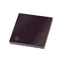
ispPAC-POWR6AT6-01N32I Lattice, ispPAC-POWR6AT6-01N32I Datasheet - Page 4

ispPAC-POWR6AT6-01N32I
Manufacturer Part Number
ispPAC-POWR6AT6-01N32I
Description
Supervisory Circuits Prec. Prog. Pwr Sppl y Seq. Mon. Trim I
Manufacturer
Lattice
Datasheet
1.ISPPAC-POWR6AT6-01NN32I.pdf
(35 pages)
Specifications of ispPAC-POWR6AT6-01N32I
Number Of Voltages Monitored
6
Output Type
Open Collector / Drain
Manual Reset
Not Resettable
Watchdog
No Watchdog
Power-up Reset Delay (typ)
500 ms
Supply Voltage (max)
3.96 V
Supply Voltage (min)
2.8 V
Supply Current (typ)
10 mA
Mounting Style
SMD/SMT
Package / Case
QFN-32
Lead Free Status / Rohs Status
Lead free / RoHS Compliant
Lattice Semiconductor
Pin Descriptions (Cont.)
1. Open-drain outputs require an external pull-up resistor to a supply.
2. Normally asserted low, but can be programmed to assert high (open) if desired.
3. The VMONxGS inputs are the ground sense line for each given VMON pin. The VMON input pins along with the VMONxGS ground sense
4. VCCA and VCCD pins must be connected together on the circuit board.
Number
Die Pad
pins implement a differential pair for each voltage monitor to allow remote sense at the load. VMONxGS lines must be connected and are
not to exceed -0.3V to +0.3V in reference to the GND pin.
10
11
1
3
5
4
TDO
TCK
TMS
TDI
SCL
SDA
NC
Name
Digital Output
Digital Input
Digital Input
Digital Input
Digital Input
Digital I/O
No Connection
Pin Type
Voltage Range
3-4
JTAG Test Data Out
JTAG Test Clock Input
JTAG Test Mode Select; Internal Pullup
JTAG Test Data In; Internal Pullup
I
I
No Internal Connection
2
2
C Serial Clock Input
C Serial Data, Bi-directional Pin
ispPAC-POWR6AT6 Data Sheet
Description


