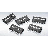
FM3264-G Ramtron, FM3264-G Datasheet - Page 13

FM3264-G
Manufacturer Part Number
FM3264-G
Description
Supervisory Circuits 64K w/Pwr Mon WDT Bat Sw Pwr Fail
Manufacturer
Ramtron
Datasheet
1.FM3264-G.pdf
(21 pages)
Specifications of FM3264-G
Number Of Voltages Monitored
4
Monitored Voltage
2.6 V or 2.9 V or 3.9 V or 4.4 V
Output Type
Active Low or Bidirectional
Manual Reset
Resettable
Watchdog
Watchdog
Battery Backup Switching
Backup
Power-up Reset Delay (typ)
200 ms
Supply Voltage (max)
5.5 V
Supply Voltage (min)
2.7 V
Supply Current (typ)
1500 uA
Maximum Operating Temperature
+ 85 C
Mounting Style
SMD/SMT
Package / Case
SOIC-14
Minimum Operating Temperature
- 40 C
Power Fail Detection
Yes
Lead Free Status / Rohs Status
Lead free / RoHS Compliant
Available stocks
Company
Part Number
Manufacturer
Quantity
Price
Company:
Part Number:
FM3264-GTR
Manufacturer:
CYPRESS
Quantity:
2 500
or Stop condition prior to the 8
below illustrate a single- and multiple-writes to
Memory Read Operation
There are two types of memory read operations. They
are current address read and selective address read. In
a current address read, the FM32xx uses the internal
address latch to supply the address. In a selective
read, the user performs a procedure to first set the
address to a specific value.
Current Address & Sequential Read
As mentioned above the FM32xx uses an internal
latch to supply the address for a read operation. A
current address read uses the existing value in the
address latch as a starting place for the read
operation. The system reads from the address
immediately following that of the last operation.
To perform a current address read, the bus master
supplies a slave address with the LSB set to 1. This
indicates that a read operation is requested. After
receiving the complete device address, the FM32xx
will begin shifting data out from the current address
on the next clock. The current address is the value
held in the internal address latch.
Beginning with the current address, the bus master
can read any number of bytes. Thus, a sequential read
is simply a current address read with multiple byte
transfers. After each byte the internal address counter
will be incremented.
Rev. 3.1
July 2010
By FM32xx
By FM32xx
By Master
By Master
Start
S
Start
S
Slave Address
Slave Address
0
th
A
data bit. The figures
Figure 11. Multiple Byte Memory Write
Address & Data
Address MSB
0
Figure 10. Single Byte Memory Write
A
Address & Data
Acknowledge
Address MSB
A
Address LSB
Acknowledge
memory.
There are four ways to terminate a read operation.
Failing to properly terminate the read will most likely
create a bus contention as the FM32xx attempts to
read out additional data onto the bus. The four valid
methods follow.
1.
2.
3.
4.
If the internal address reaches the top of memory, it
will wrap around to 0000h on the next read cycle.
The figures below show the proper operation for
current address reads.
Selective (Random) Read
There is a simple technique that allows a user to
select a random address location as the starting point
for a read operation. This involves using the first
A
Each time the bus master acknowledges a byte,
this indicates that the FM32xx should read out
the next sequential byte.
The bus master issues a NACK in the 9
cycle and a Stop in the 10
illustrated in the diagrams below and is
preferred.
The bus master issues a NACK in the 9
cycle and a Start in the 10
The bus master issues a Stop in the 9
cycle.
The bus master issues a Start in the 9
cycle.
Address LSB
A
Data Byte
A
A
th
.
th
Data Byte
clock cycle. This is
FM3204/16/64/256
Data Byte
Page 13 of 21
th
th
th
th
A
clock
clock
clock
clock
A
Stop
Stop
P
P


