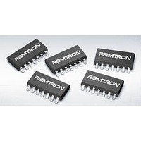
FM3264-G Ramtron, FM3264-G Datasheet - Page 15

FM3264-G
Manufacturer Part Number
FM3264-G
Description
Supervisory Circuits 64K w/Pwr Mon WDT Bat Sw Pwr Fail
Manufacturer
Ramtron
Datasheet
1.FM3264-G.pdf
(21 pages)
Specifications of FM3264-G
Number Of Voltages Monitored
4
Monitored Voltage
2.6 V or 2.9 V or 3.9 V or 4.4 V
Output Type
Active Low or Bidirectional
Manual Reset
Resettable
Watchdog
Watchdog
Battery Backup Switching
Backup
Power-up Reset Delay (typ)
200 ms
Supply Voltage (max)
5.5 V
Supply Voltage (min)
2.7 V
Supply Current (typ)
1500 uA
Maximum Operating Temperature
+ 85 C
Mounting Style
SMD/SMT
Package / Case
SOIC-14
Minimum Operating Temperature
- 40 C
Power Fail Detection
Yes
Lead Free Status / Rohs Status
Lead free / RoHS Compliant
Available stocks
Company
Part Number
Manufacturer
Quantity
Price
Company:
Part Number:
FM3264-GTR
Manufacturer:
CYPRESS
Quantity:
2 500
Addressing FRAM Array in the FM32xx Family
The FM32xx family includes 256Kb, 64Kb, 16Kb, and 4Kb memory densities. The following 2-byte address field is
shown for each density.
Table 4. Two-Byte Memory Address
Rev. 3.1
July 2010
Part #
By Master
By FM32xx
By FM32xx
By Master
FM32256
FM3264
FM3216
FM3204
Start
S
Slave Address
* Although not required, it is recommended that A5-A7 in the Register Address byte are
Start
x
x
x
x
S
A14
x
x
x
0
A
Slave Address
zeros in order to preserve compatibility with future devices.
A13
x
x
x
Figure 14. Selective (Random) Memory Read
Address MSB
1
Address
st
Address Byte
A12
A12
x
x
Figure 15. Byte Register Write
A11
A11
x
x
0
A
A
A10
A10
A10
x
Address LSB
0 0 0
Acknowledge
Address & Data
A9
A9
A9
x
A8
A8
A8
A8
Address
A
Start
S
A7
A7
A7
A7
Acknowledge
Slave Address
Address
A6
A6
A6
A6
A
A5
A5
A5
A5
2
nd
1
Address Byte
A
Data Byte
A4
A4
A4
A4
A3
A3
A3
A3
Data Byte
FM3204/16/64/256
Data
A2
A2
A2
A2
Acknowledge
A1
A1
A1
A1
Page 15 of 21
No
A
1 P
A0
A0
A0
A0
P
Stop
Stop


