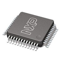
LPC11C22FBD48/301,151 NXP Semiconductors, LPC11C22FBD48/301,151 Datasheet - Page 50

LPC11C22FBD48/301,151
Manufacturer Part Number
LPC11C22FBD48/301,151
Description
Microcontrollers (MCU) CAN Transceiver MCU 16K Flash
Manufacturer
NXP Semiconductors
Datasheet
1.LPC11C22FBD48301151.pdf
(62 pages)
Specifications of LPC11C22FBD48/301,151
Processor Series
LPC11Cx2
Core
ARM Cortex-M0
Data Bus Width
32 bit
Program Memory Type
Flash
Program Memory Size
16 KB
Data Ram Size
8 KB
Interface Type
CAN, I2C, SPI, UART
Maximum Clock Frequency
50 MHz
Number Of Programmable I/os
36
Number Of Timers
4
Operating Supply Voltage
3.3 V
Maximum Operating Temperature
+ 85 C
Mounting Style
SMD/SMT
Development Tools By Supplier
OM13012,598
Minimum Operating Temperature
- 40 C
Lead Free Status / Rohs Status
Details
Other names
935294284151
NXP Semiconductors
11. Application information
LPC11CX2_CX4
Product data sheet
11.1 ADC usage notes
11.2 XTAL input
The following guidelines show how to increase the performance of the ADC in a noisy
environment beyond the ADC specifications listed in
The input voltage to the on-chip oscillators is limited to 1.8 V. If the oscillator is driven by a
clock in slave mode, it is recommended that the input be coupled through a capacitor with
C
capacitor to ground C
mode, a minimum of 200 mv (RMS) is needed.
In slave mode the input clock signal should be coupled by means of a capacitor of 100 pF
(Figure
corresponds to a square wave signal with a signal swing of between 280 mV and 1.4 V.
The XTALOUT pin in this configuration can be left unconnected.
External components and models used in oscillation mode are shown in
Table 19
and the capacitances C
fundamental mode oscillation (the fundamental frequency is represented by L, C
R
not be larger than 7 pF. Parameters F
manufacturer (see
Fig 23. Slave mode operation of the on-chip oscillator
•
•
•
•
i
S
= 100 pF. To limit the input voltage to the specified range, choose an additional
). Capacitance C
The ADC input trace must be short and as close as possible to the LPC11Cx2/Cx4
chip.
The ADC input traces must be shielded from fast switching digital signals and noisy
power supply lines.
Because the ADC and the digital core share the same power supply, the power supply
line must be adequately filtered.
To improve the ADC performance in a very noisy environment, put the device in Sleep
mode during the ADC conversion.
23), with an amplitude between 200 mv (RMS) and 1000 mv (RMS). This
and
Table
All information provided in this document is subject to legal disclaimers.
Table
P
20. Since the feedback resistance is integrated on chip, only a crystal
in
g
which attenuates the input voltage by a factor C
Figure 24
X1
Rev. 3 — 27 June 2011
19).
and C
X2
represents the parallel package capacitance and should
need to be connected externally in case of
OSC
XTALIN
LPC1xxx
C i
100 pF
, C
L
, R
S
002aae788
32-bit ARM Cortex-M0 microcontroller
C g
and C
Table
P
are supplied by the crystal
LPC11Cx2/Cx4
7:
i
/(C
© NXP B.V. 2011. All rights reserved.
Figure 24
i
+ C
g
). In slave
L
and
and in
50 of 62


