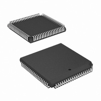
HSP43220JC-25Z Intersil, HSP43220JC-25Z Datasheet - Page 3

HSP43220JC-25Z
Manufacturer Part Number
HSP43220JC-25Z
Description
IC DECIMATING DGTL FILTER 84PLCC
Manufacturer
Intersil
Datasheet
1.HSP43220JC-25Z.pdf
(21 pages)
Specifications of HSP43220JC-25Z
Filter Type
Digital
Number Of Filters
4
Voltage - Supply
4.75 V ~ 5.25 V
Mounting Type
Surface Mount
Package / Case
84-PLCC
Lead Free Status / RoHS Status
Lead free / RoHS Compliant
Frequency - Cutoff Or Center
-
Max-order
-
Available stocks
Company
Part Number
Manufacturer
Quantity
Price
Pin Description
The HDF
The first filter section is called the High Order Decimation Filter
(HDF) and is optimized to perform decimation by large factors.
It implements a low pass filter using only adders and delay
elements instead of a large number of multiplier/ accumulators
that would be required using a standard FIR filter.
The HDF is divided into 4 sections: the HDF filter section,
the clock divider, the control register logic and the start logic
(Figure 1).
DATA_IN0-15
C_BUS0-15
DATA_OUT
DATA_RDY
STARTOUT
OUT_SELH
ASTARTIN
OUT_ENP
OUT_ENX
STARTIN
RESET
A0, A1
NAME
0-23
WR
CS
TYPE
O
O
O
I
I
I
I
I
I
I
I
I
I
I
Input Data Bus. This bus is used to provide the 16-bit input data to the HSP43220. The data must be provided in a
synchronous fashion, and is latched on the rising edge of the CK_IN signal. The data bus is in 2's complement fractional
format. Bit 15 is the MSB.
Control Input Bus. This input bus is used to load all the filter parameters. The pins WR, CS and A0, A1 are used to select
the destination of the data on the Control bus and write the Control bus data into the appropriate register as selected by A0
and A1
Output Data Bus. This 24-Bit output port is used to provide the filtered result in 2's complement format. The upper 8 bits of
the output, DATA_OUT16-23 will provide extension or growth bits depending on the state of OUT_SELH and whether the
FIR has been put in bypass mode. Output bits DATA_OUT0-15 will provide bits 20 through 2-15 when the FIR is not
bypassed and will provide the bits 2-16 through 2-31 when the FIR is in bypass mode.
An active high output strobe that is synchronous with FIR_CK that indicates that the result of the just completed FIR cycle
is available on the data bus.
RESET is an asynchronous signal which requires that the input clocks CK_IN and FIR_CK are active when RESET is
asserted. RESET disables the clock divider and clears all of the internal data registers in the HDF. The FIR filter data path
is not initialized. The control register bits that are cleared are F_BYP, H_STAGES, and H_DRATE. The F_DIS bit is set. In
order to guarantee consistent operation of the part, the user must reset the DDF after power-up.
Write Strobe. WR is used for loading the internal registers of the HSP43220. When CS and WR are asserted, the rising edge of
WR will latch the C_BUS0-15 data into the register specified by A0 and A1.
Chip Select. The Chip Select input enables loading of the internal registers. When CS and WR are low, the A0 and A1 address
lines are decoded to determine the destination of the data on C_BUS0-15. The rising edge of WR then loads the appropriate
register as specified by A0 and A1.
Control Register Address. These lines are decoded to determine which control register is the destination for the data on
C_BUS0-15. Register loading is controlled by the A0 and A1, WR and CS inputs.
ASTARTIN is an asynchronous signal which is sampled on the rising edge of CK_IN. It is used to put the DDF in operational
mode. ASTARTIN is internally synchronized to CK_IN and is used to generate STARTOUT.
STARTOUT is a pulse generated from the internally synchronized version of ASTARTIN. It is provided as an output for use
in multi-chip configurations to synchronously start multiple HSP43220's. The width of STARTOUT is equal to the period of
CK_IN.
STARTIN is a Synchronous Input. A high to low transition of this signal is required to start the part. STARTIN is sampled on
the rising edge of CK_IN. This synchronous signal can be used to start single or multiple HSP43220's.
Output Select. The OUT_SELH input controls which bits are provided at output pins DATA_OUT16-23. A HIGH on this control
line selects bits 28 through 21 from the accumulator output. A LOW on this control line selects bits 2-16 through 2-23 from
the accumulator output. Processing is not interrupted by this pin.
Output Enable. The OUT_ENP input controls the state of the lower 16 bits of the output data bus, DATA_OUT0-15. A LOW on
this control line enables the lower 16 bits of the output bus. When OUT_ENP is HIGH, the output drivers are in the high
impedance state. Processing is not interrupted by this pin.
Output Enable. The OUT_ENX input controls the state of the upper 8 bits of the output data bus, DATA_OUT16-23. A LOW
on this control line enables the upper 8 bits of the output bus. When OUT_ENX is HIGH, the output drivers are in the high
impedance state. Processing is not interrupted by this pin.
(Continued)
3
HSP43220
DESCRIPTION
Data Shifter
After being latched into the Input Register the data enters the
Data Shifter. The data is positioned at the output of the shifter
to prevent errors due to overflow occurring at the output of the
HDF. The number of bits to shift is controlled by H_GROWTH.
October 10, 2008
FN2486.10


