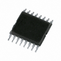
PCA9538PW,118 NXP Semiconductors, PCA9538PW,118 Datasheet - Page 8

PCA9538PW,118
Manufacturer Part Number
PCA9538PW,118
Description
IC I/O EXPANDER I2C 8B 16TSSOP
Manufacturer
NXP Semiconductors
Datasheet
1.PCA9538BS118.pdf
(28 pages)
Specifications of PCA9538PW,118
Package / Case
16-TSSOP
Interface
I²C, SMBus
Number Of I /o
8
Interrupt Output
Yes
Frequency - Clock
400kHz
Voltage - Supply
2.3 V ~ 5.5 V
Operating Temperature
-40°C ~ 85°C
Mounting Type
Surface Mount
Includes
POR
Logic Family
PCA9538
Number Of Lines (input / Output)
8.0 / 8.0
Operating Supply Voltage
2.3 V to 5.5 V
Power Dissipation
200 mW
Operating Temperature Range
- 40 C to + 85 C
Input Voltage
5 V
Logic Type
I2C, SMBus
Maximum Clock Frequency
400 KHz
Mounting Style
SMD/SMT
Number Of Input Lines
8.0
Number Of Output Lines
8.0
Output Current
50 mA
Output Voltage
5 V
Lead Free Status / RoHS Status
Lead free / RoHS Compliant
For Use With
568-3615 - DEMO BOARD I2C
Lead Free Status / Rohs Status
Lead free / RoHS Compliant
Other names
568-1840-2
935277419118
PCA9538PW-T
935277419118
PCA9538PW-T
Available stocks
Company
Part Number
Manufacturer
Quantity
Price
Company:
Part Number:
PCA9538PW,118
Manufacturer:
TI
Quantity:
2 500
NXP Semiconductors
PCA9538_5
Product data sheet
6.6 I/O port
When an I/O is configured as an input, FETs Q1 and Q2 are off, creating a
high-impedance input. The input voltage may be raised above V
If the I/O is configured as an output, then either Q1 or Q2 is enabled, depending on the
state of the Output Port register. Care should be exercised if an external voltage is applied
to an I/O configured as an output because of the low-impedance paths that exist between
the pin and either V
Fig 6.
configuration
write polarity
shift register
shift register
shift register
write pulse
read pulse
data from
data from
data from
pulse
pulse
write
Remark: At power-on reset, all registers return to default values.
Simplified schematic of IO0 to IO7
configuration
register
D
CK
8-bit I
FF
DD
Q
Q
or V
2
Rev. 05 — 28 May 2009
C-bus and SMBus low power I/O port with interrupt and reset
SS
.
output port
register
D
CK
FF
Q
input port
register
polarity inversion
register
D
CK
D
CK
FF
FF
Q
Q
Q1
DD
to a maximum of 5.5 V.
Q2
PCA9538
© NXP B.V. 2009. All rights reserved.
output port
register data
V
I/O pin
V
input port
register data
to INT
polarity
inversion
register data
DD
SS
002aad723
8 of 28


