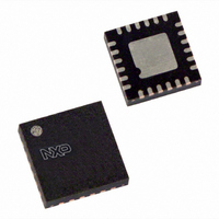
PCA9539BS,118 NXP Semiconductors, PCA9539BS,118 Datasheet - Page 14

PCA9539BS,118
Manufacturer Part Number
PCA9539BS,118
Description
IC I/O EXPANDER I2C 16B 24HVQFN
Manufacturer
NXP Semiconductors
Datasheet
1.PCA9539BS118.pdf
(31 pages)
Specifications of PCA9539BS,118
Package / Case
24-VQFN Exposed Pad, 24-HVQFN, 24-SQFN, 24-DHVQFN
Interface
I²C, SMBus
Number Of I /o
16
Interrupt Output
Yes
Frequency - Clock
400kHz
Voltage - Supply
2.3 V ~ 5.5 V
Operating Temperature
-40°C ~ 85°C
Mounting Type
Surface Mount
Includes
POR
Logic Family
PCA9539
Number Of Lines (input / Output)
16.0 / 16.0
Operating Supply Voltage
2.3 V to 5.5 V
Power Dissipation
200 mW
Operating Temperature Range
- 40 C to + 85 C
Input Voltage
5 V
Logic Type
I2C, SMBus
Maximum Clock Frequency
400 KHz
Mounting Style
SMD/SMT
Number Of Input Lines
16.0
Number Of Output Lines
16.0
Output Current
50 mA
Output Voltage
5 V
Lead Free Status / RoHS Status
Lead free / RoHS Compliant
Lead Free Status / RoHS Status
Lead free / RoHS Compliant, Lead free / RoHS Compliant
Other names
568-1841-2
935277296118
PCA9539BS-T
935277296118
PCA9539BS-T
Available stocks
Company
Part Number
Manufacturer
Quantity
Price
Company:
Part Number:
PCA9539BS,118
Manufacturer:
MICREL
Quantity:
1 001
NXP Semiconductors
7. Characteristics of the I
PCA9539_PCA9539R_5
Product data sheet
6.6.3 Interrupt output
7.1.1 START and STOP conditions
7.1 Bit transfer
The open-drain interrupt output is activated when one of the port pins change state and
the pin is configured as an input. The interrupt is deactivated when the input returns to its
previous state or the Input port register is read (see
output cannot cause an interrupt. Since each 8-bit port is read independently, the interrupt
caused by Port 0 will not be cleared by a read of Port 1 or the other way around.
Remark: Changing an I/O from an output to an input may cause a false interrupt to occur
if the state of the pin does not match the contents of the Input port register.
The I
lines are a serial data line (SDA) and a serial clock line (SCL). Both lines must be
connected to a positive supply via a pull-up resistor when connected to the output stages
of a device. Data transfer may be initiated only when the bus is not busy.
One data bit is transferred during each clock pulse. The data on the SDA line must remain
stable during the HIGH period of the clock pulse as changes in the data line at this time
will be interpreted as control signals (see
Both data and clock lines remain HIGH when the bus is not busy. A HIGH-to-LOW
transition of the data line while the clock is HIGH is defined as the START condition (S). A
LOW-to-HIGH transition of the data line while the clock is HIGH is defined as the STOP
condition (P) (see
Fig 12. Bit transfer
Fig 13. Definition of START and STOP conditions
2
C-bus is for 2-way, 2-line communication between different ICs or modules. The two
SDA
SCL
START condition
16-bit I
2
SDA
SCL
Figure
C-bus
S
2
Rev. 05 — 28 July 2008
C-bus and SMBus low power I/O port with interrupt and reset
13).
data valid
data line
stable;
Figure
PCA9539; PCA9539R
allowed
change
of data
12).
Figure
10). A pin configured as an
STOP condition
mba607
P
© NXP B.V. 2008. All rights reserved.
mba608
SDA
SCL
14 of 31


