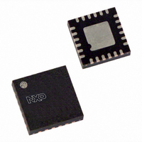
PCA9539BS,118 NXP Semiconductors, PCA9539BS,118 Datasheet - Page 8

PCA9539BS,118
Manufacturer Part Number
PCA9539BS,118
Description
IC I/O EXPANDER I2C 16B 24HVQFN
Manufacturer
NXP Semiconductors
Datasheet
1.PCA9539BS118.pdf
(31 pages)
Specifications of PCA9539BS,118
Package / Case
24-VQFN Exposed Pad, 24-HVQFN, 24-SQFN, 24-DHVQFN
Interface
I²C, SMBus
Number Of I /o
16
Interrupt Output
Yes
Frequency - Clock
400kHz
Voltage - Supply
2.3 V ~ 5.5 V
Operating Temperature
-40°C ~ 85°C
Mounting Type
Surface Mount
Includes
POR
Logic Family
PCA9539
Number Of Lines (input / Output)
16.0 / 16.0
Operating Supply Voltage
2.3 V to 5.5 V
Power Dissipation
200 mW
Operating Temperature Range
- 40 C to + 85 C
Input Voltage
5 V
Logic Type
I2C, SMBus
Maximum Clock Frequency
400 KHz
Mounting Style
SMD/SMT
Number Of Input Lines
16.0
Number Of Output Lines
16.0
Output Current
50 mA
Output Voltage
5 V
Lead Free Status / RoHS Status
Lead free / RoHS Compliant
Lead Free Status / RoHS Status
Lead free / RoHS Compliant, Lead free / RoHS Compliant
Other names
568-1841-2
935277296118
PCA9539BS-T
935277296118
PCA9539BS-T
Available stocks
Company
Part Number
Manufacturer
Quantity
Price
Company:
Part Number:
PCA9539BS,118
Manufacturer:
MICREL
Quantity:
1 001
NXP Semiconductors
PCA9539_PCA9539R_5
Product data sheet
6.2.5 Registers 6 and 7: Configuration registers
6.3 Power-on reset
6.4 RESET input
6.5 I/O port
This register configures the directions of the I/O pins. If a bit in this register is set (written
with ‘1’), the corresponding port pin is enabled as an input with high-impedance output
driver. If a bit in this register is cleared (written with ‘0’), the corresponding port pin is
enabled as an output. At reset, the device's ports are inputs.
Table 11.
Table 12.
When power is applied to V
in a reset condition until V
released and the PCA9539; PCA9539R registers and SMBus state machine will initialize
to their default states. Thereafter, V
For a power reset cycle, V
operating voltage.
A reset can be accomplished by holding the RESET pin LOW for a minimum of t
the PCA9539 the registers and SMBus/I
state until the RESET input is once again HIGH. This input typically requires a pull-up to
V
general-purpose registers remain unchanged. Using the PCA9539R hardware reset pin
will only reset the I
I
any lines in their previously defined state and not cause system errors while the I
being restored.
When an I/O is configured as an input, FETs Q1 and Q2 are off, creating a
high-impedance input. The input voltage may be raised above V
If the I/O is configured as an output, then either Q1 or Q2 is on, depending on the state of
the Output port register. Care should be exercised if an external voltage is applied to an
I/O configured as an output because of the low-impedance path that exists between the
pin and either V
Bit
Symbol
Default
Bit
Symbol
Default
2
DD
C-bus. This allows the I/O pins to retain their last configured state so that they can keep
. In the PCA9539R, only the device state machine is initialized. The internal
Configuration port 0 register
Configuration port 1 register
C0.7
C1.7
7
1
7
1
16-bit I
DD
2
or V
C-bus interface should it be stuck LOW to regain access to the
C0.6
C1.6
2
SS
Rev. 05 — 28 July 2008
C-bus and SMBus low power I/O port with interrupt and reset
6
1
6
1
.
DD
DD
DD
has reached V
must be lowered below 0.2 V and then restored to the
, an internal power-on reset holds the PCA9539; PCA9539R
C0.5
C1.5
5
1
5
1
DD
must be lowered below 0.2 V to reset the device.
2
C-bus state machine will be held in their default
C0.4
C1.4
POR
4
1
4
1
PCA9539; PCA9539R
. At that point, the reset condition is
C0.3
C1.3
3
1
3
1
C0.2
C1.2
DD
2
2
1
1
to a maximum of 5.5 V.
© NXP B.V. 2008. All rights reserved.
C0.1
C1.1
1
1
1
1
2
w(rst)
C-bus is
C0.0
C1.0
0
1
0
1
8 of 31
. In


