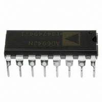
AD694JNZ Analog Devices Inc, AD694JNZ Datasheet - Page 2

AD694JNZ
Manufacturer Part Number
AD694JNZ
Description
IC TRANSMITTER 4-20MA 16-DIP
Manufacturer
Analog Devices Inc
Type
Current Transmitterr
Datasheet
1.AD694JNZ.pdf
(16 pages)
Specifications of AD694JNZ
Input Type
Voltage
Output Type
Voltage
Current - Supply
23mA
Mounting Type
Through Hole
Package / Case
16-DIP (0.300", 7.62mm)
Number Of Channels
1
Number Of Elements
3
Power Supply Requirement
Single
Common Mode Rejection Ratio
80dB
Voltage Gain Db
93.98dB
Input Resistance
5@24VMohm
Input Offset Voltage
0.5@24VmV
Input Bias Current
0.005@24V@-40C TO 85nA
Single Supply Voltage (typ)
5/9/12/15/18/24/28V
Dual Supply Voltage (typ)
Not RequiredV
Power Supply Rejection Ratio
80dB
Rail/rail I/o Type
No
Single Supply Voltage (min)
4.5V
Single Supply Voltage (max)
36V
Dual Supply Voltage (min)
Not RequiredV
Dual Supply Voltage (max)
Not RequiredV
Operating Temp Range
0C to 70C
Operating Temperature Classification
Commercial
Mounting
Through Hole
Pin Count
16
Package Type
PDIP
No. Of Amplifiers
4
Bandwidth
300kHz
Amplifier Output
Differential
Cmrr
90dB
Supply Voltage Range
4.5V To 36V, 12.5V To 36V
Supply Current
2mA
Rohs Compliant
Yes
Lead Free Status / RoHS Status
Lead free / RoHS Compliant
Interface
-
Lead Free Status / Rohs Status
RoHS Compliant part
Electrostatic Device
Available stocks
Company
Part Number
Manufacturer
Quantity
Price
Company:
Part Number:
AD694JNZ
Manufacturer:
ALTERA
Quantity:
3 000
Part Number:
AD694JNZ
Manufacturer:
ADI/亚德诺
Quantity:
20 000
AD694–SPECIFICATIONS
Model
INPUT CHARACTERISTICS
OUTPUT CHARACTERISTICS
SPAN AND ZERO ACCURACY
VOLTAGE REFERENCE
ALARM CHARACTERISTICS
POWER REQUIREMENTS
TEMPERATURE RANGE
Input Voltage Range
Input Bias Current
Input Impedance
Operating Current Range
Specified Performance
Output Voltage Compliance
Output Impedance, 4–20 mA
Current Limit (@ 2 × FS Overdrive
Slew Rate
4 mA Offset Error @ 0 V Input
Span
4 mA On: Max Pin 9 Voltage
4 mA Off: Min Pin 9 Voltage
Output Voltage: 10 V Reference
Output Voltage: 2 V Reference
vs. Load, V
vs. Supply, V
Output Current
V
Leakage Current
Alarm Pin Current (Pin 10)
Specified Performance
Operating Range
Quiescent Current, 4 mA Off
Specified Performance
Operating
CE(SAT)
Either Input, T
Offset Current, T
Offset Current Drift
Error from 4.000 mA, 4 mA On
Error from 0.000 mA, 4 mA Off
T
vs. Supply (2 V Span/10 V Span)
Trim Range, 4 mA Zero
Nominal Transfer Function
Transfer Function Error from Nom,
T
Source
Sink
2 V FS, V
2 V, 10 V FS, V
MIN
MIN
Input FS = 2 V
Input FS = 10 V
Input FS = 2 V, 10 V
T
vs. Supply
Nonlinearity
MIN
to T
to T
@ 2.5 mA
to T
REF
REF
MAX
MAX
REF
MAX
= 2 V, 10 V
= 2 V
4
= 2 V, 10 V
3
MIN
REF
MIN
to T
= 2 V, 10 V
5
to T
AD694AQ/BQ/AR/BR –40
AD694JN
AD694AQ/BQ/AR/BR –55
AD694JN
MAX
MAX
2
1
Min
–0.2
5
0
4
V
40.0
24
0
2.0
3.0
9.960
1.992
5
4.5
12.5
0
–40
(@ +25 C, R
S
–36 V
AD694JN/AQ/AR
Typ
V
1.5
± 0.1
± 1.0
50.0
1.3
± 10
+10
± 10
0.3/0.05
8.0
1.6
± 0.1
± 0.002
± 0.001
± 0.005
2.5
10.000
2.000
30
0.15
± 0.001
0.2
0.35
20
24
1.5
L
S
–2–
= 250
–2.0 V
, and V
Max
V
5
± 5.0
23
20
V
44
+20
0.8/0.4
± 0.005
0.8
10.040
50
0.50
36
36
2.0
4.8
2.008
+85
+70
+125
+85
S
S
1
20
40
0.3
0.005
0.015
0.005
1
–2.5 V –0.2
–2 V
S
= +24 V, unless otherwise noted.)
Min
5
0
4
V
40.0
24
0
2.0
3.0
9.980
1.996
5
4.5
12.5
–40
0
–55
–40
S
–36 V
AD694BQ/BR
Typ
V
1.5
± 0.1
± 1.0
50.0
1.3
± 5
+5
± 5
0.3/0.05
8.0
1.6
± 0.05
± 0.001
± 0.001
± 0.001
2.5
10.000
2.000
20
0.15
± 0.001
0.2
0.35
20
24
1.5
S
–2.0 V V
5
23
20
V
44
0.8
30
0.50
2.0
Max
± 5.0
+10
0.8/0.4
4.8
10.020
2.004
36
36
+85
+70
+125
+85
S
S
1
10
20
0.15
0.0025 % of Span/°C
0.005
0.005
0.005
1
–2.5 V V
2 V
Unit
nA
nA
pA/°C
MΩ
mA
mA
V
MΩ
mA
mA/µs
µA
µA
µA
µA/V
mA
mA/V
mA/V
% of Span
% of Span/V
% of Span
V
V
V
V
ppm/°C
mV/mA
%/V
mA
mA
V
µA
mA
V
V
V
mA
°C
°C
°C
°C
REV. B


