AD694JNZ Analog Devices Inc, AD694JNZ Datasheet - Page 4
AD694JNZ
Manufacturer Part Number
AD694JNZ
Description
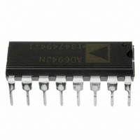
IC TRANSMITTER 4-20MA 16-DIP
Manufacturer
Analog Devices Inc
Type
Current Transmitterr
Datasheet
1.AD694JNZ.pdf
(16 pages)
Specifications of AD694JNZ
Input Type
Voltage
Output Type
Voltage
Current - Supply
23mA
Mounting Type
Through Hole
Package / Case
16-DIP (0.300", 7.62mm)
Number Of Channels
1
Number Of Elements
3
Power Supply Requirement
Single
Common Mode Rejection Ratio
80dB
Voltage Gain Db
93.98dB
Input Resistance
5@24VMohm
Input Offset Voltage
0.5@24VmV
Input Bias Current
0.005@24V@-40C TO 85nA
Single Supply Voltage (typ)
5/9/12/15/18/24/28V
Dual Supply Voltage (typ)
Not RequiredV
Power Supply Rejection Ratio
80dB
Rail/rail I/o Type
No
Single Supply Voltage (min)
4.5V
Single Supply Voltage (max)
36V
Dual Supply Voltage (min)
Not RequiredV
Dual Supply Voltage (max)
Not RequiredV
Operating Temp Range
0C to 70C
Operating Temperature Classification
Commercial
Mounting
Through Hole
Pin Count
16
Package Type
PDIP
No. Of Amplifiers
4
Bandwidth
300kHz
Amplifier Output
Differential
Cmrr
90dB
Supply Voltage Range
4.5V To 36V, 12.5V To 36V
Supply Current
2mA
Rohs Compliant
Yes
Lead Free Status / RoHS Status
Lead free / RoHS Compliant
Interface
-
Lead Free Status / Rohs Status
RoHS Compliant part
Electrostatic Device
Available stocks
Company
Part Number
Manufacturer
Quantity
Price
Company:

Part Number:
AD694JNZ
Manufacturer:
ALTERA
Quantity:
3 000
Part Number:
AD694JNZ
Manufacturer:
ADI/亚德诺
Quantity:
20 000


AD694
Typical Minimum Supply Voltage vs. Temperature for 2 V
and 10 V Full Scale
Voltage Reference Power Supply Rejection
I
OUT
: Voltage Compliance vs. Temperature
Maximum R
L
vs. Supply Voltage
–4–
FUNCTIONAL DESCRIPTION
The operation of the AD694 can best be understood by dividing
the circuit into three functional parts (see Figure 1). First, a
single supply input amplifier buffers the high level, single-ended
input signal. The buffer amplifier drives the second section, a
voltage to current (V/I) converter, that makes a 0 to 16 mA sig-
nal dependent current.
The third section, a voltage reference and offset generator, is re-
sponsible for providing the 4 mA offset current signal.
BUFFER AMPLIFIER
The buffer amplifier is a single supply amplifier that may be
used as a unity gain buffer, an output amplifier for a current
output DAC, or as a gain block to amplify low level signals. The
amplifier’s PNP input stage has a common-mode range that ex-
tends from a few hundred mV below ground to within 2.5 V of
V
The output range extends from about 1 mV above common to
within 2.5 V of V
The amplifier can source a maximum load of 5 kΩ, but can sink
only as much as its internal 10 kΩ pulldown resistor allows.
V/I CONVERTER
The ground referenced, input signal from the buffer amplifier is
converted to a 0 to 0.8 mA current by A2 and level shifted to
the positive supply. A current mirror then multiplies this signal
by a factor of 20 to make the signal current of 0 to 16 mA. This
technique allows the output stage to drive a load to within 2 V
of the positive supply (V
Pin 1 across resistors R1 and R2 by driving the Darlington tran-
sistor, Q2. The high gain Darlington transmits the resistor cur-
rent to its collector and to R3 (900 Ω). A3 forces the level
shifted signal across the 45 Ω resistor to get a current gain of 20.
The transfer function of the V/I stage is therefore:
resulting in a 0-16 mA output swing for a 0–10 V input. Tying
Pin 4 (2 V FS) to ground shorts out R2 and results in a 2 V
full-scale input for a 16 mA output span.
The output stage of the V/I converter is of a unique design that
allows the I
strate) potential of the device. The output transistor can always
drive a load to a point 36 V below the positive supply (V
S
. The Class A output of the amplifier appears at Pin 1 (FB).
OUT
Figure 1. Functional Block Diagram
I
OUT
pin to drive a load below the common (sub-
S
when the amplifier is operated as a follower.
=
20
×
S
). Amplifier A2 forces the voltage at
V
PIN1
/
(
R1
+
R2
)
S
REV. B
). An
Related parts for AD694JNZ
Image
Part Number
Description
Manufacturer
Datasheet
Request
R

Part Number:
Description:
±1.7g Dual-Axis IMEMS Accelerometer Evaluation Board
Manufacturer:
Analog Devices Inc
Datasheet:

Part Number:
Description:
Inertial Sensor Evaluation System
Manufacturer:
Analog Devices Inc
Datasheet:
Part Number:
Description:
Manufacturer:
Analog Devices Inc
Datasheet:
Part Number:
Description:
Manufacturer:
Analog Devices Inc
Datasheet:
Part Number:
Description:
Manufacturer:
Analog Devices Inc
Datasheet:
Part Number:
Description:
Manufacturer:
Analog Devices Inc
Datasheet:
Part Number:
Description:
Manufacturer:
Analog Devices Inc
Datasheet:
Part Number:
Description:
Manufacturer:
Analog Devices Inc
Datasheet:
Part Number:
Description:
Manufacturer:
Analog Devices Inc
Datasheet:
Part Number:
Description:
Manufacturer:
Analog Devices Inc
Datasheet:
Part Number:
Description:
Manufacturer:
Analog Devices Inc
Datasheet:
Part Number:
Description:
Manufacturer:
Analog Devices Inc
Datasheet:
Part Number:
Description:
Manufacturer:
Analog Devices Inc
Datasheet: