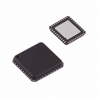
AD9948KCP Analog Devices Inc, AD9948KCP Datasheet - Page 10

AD9948KCP
Manufacturer Part Number
AD9948KCP
Description
IC CCD SIGNAL PROCESSOR 40-LFCSP
Manufacturer
Analog Devices Inc
Type
CCD Signal Processor, 10-Bitr
Datasheet
1.AD9948KCPZRL.pdf
(28 pages)
Specifications of AD9948KCP
Rohs Status
RoHS non-compliant
Input Type
Logic
Output Type
Logic
Interface
3-Wire Serial
Mounting Type
Surface Mount
Package / Case
40-LFCSP
Current - Supply
-
Available stocks
Company
Part Number
Manufacturer
Quantity
Price
Company:
Part Number:
AD9948KCP
Manufacturer:
ADI
Quantity:
210
Part Number:
AD9948KCPZ
Manufacturer:
ADI/亚德诺
Quantity:
20 000
Part Number:
AD9948KCPZRL
Manufacturer:
ADI/亚德诺
Quantity:
20 000
AD9948
Address
00
01
02
03
04
05
Address
10
11
12
13
14
15
16
17
18
19
1A
Data Bit
Content
[11:0]
[9:0]
[7:0]
[11:0]
[17:0]
[17:0]
Data Bit
Content
[0]
[0]
[0]
[11:0]
[0]
[0]
[1:0]
[0]
[1:0]
[0]
[0]
Default
Value
4
0
80
4
0
0
Default
Value
0
0
0
0
0
0
0
0
0
1
0
OPRMODE
VGAGAIN
CLAMP LEVEL
CTLMODE
PxGA GAIN01
PxGA GAIN23
TGCORE_RSTB
PREVENTUPDATE
VDHDEDGE
HBLKRETIME
CLPBLKOUT
CLPBLKEN
TEST MODE
Name
Name
SW_RST
OUT_CONTROL
UPDATE
FIELDVAL
Table III. Miscellaneous Register Map
Table II. AFE Register Map
Description
AFE Operation Modes. (See Table VIII.)
VGA Gain.
Optical Black Clamp Level.
AFE Control Modes. (See Table IX.)
PxGA Gain Registers for Color 0 [8:0] and Color 1 [17:9].
PxGA Gain Registers for Color 2 [8:0] and Color 3 [17:9].
Description
Software Reset.
1 = Reset all registers to default, then self-clear back to 0.
Output Control.
0 = Make all dc outputs inactive.
Timing Core Reset Bar.
0 = Reset TG core.
1 = Resume operation.
Serial Update.
Sets the line (HD) within the field to update serial data.
Prevents the update of the VD-Updated Registers.
1 = Prevent update.
VD/HD Active Edge.
0 = Falling edge triggered.
1 = Rising edge triggered.
Field Value Sync.
0 = Next Field 0.
1 = Next Field 1.
2/3 = Next Field 2.
Retime HBLK to Internal H1 Clock.
Preferred setting is 1. Setting to 1 will add one cycle delay to HBLK
toggle positions.
CLP/BLK Pin Output Select.
0 = CLPOB.
1 = PBLK.
2 = HBLK.
3 = Low.
Enable CLP/BLK Output.
1 = Enable.
Internal Test Mode.
Should always be set low.
–10–
REV. 0


