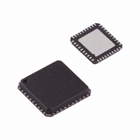
AD9948KCP Analog Devices Inc, AD9948KCP Datasheet - Page 23

AD9948KCP
Manufacturer Part Number
AD9948KCP
Description
IC CCD SIGNAL PROCESSOR 40-LFCSP
Manufacturer
Analog Devices Inc
Type
CCD Signal Processor, 10-Bitr
Datasheet
1.AD9948KCPZRL.pdf
(28 pages)
Specifications of AD9948KCP
Rohs Status
RoHS non-compliant
Input Type
Logic
Output Type
Logic
Interface
3-Wire Serial
Mounting Type
Surface Mount
Package / Case
40-LFCSP
Current - Supply
-
Available stocks
Company
Part Number
Manufacturer
Quantity
Price
Company:
Part Number:
AD9948KCP
Manufacturer:
ADI
Quantity:
210
Part Number:
AD9948KCPZ
Manufacturer:
ADI/亚德诺
Quantity:
20 000
Part Number:
AD9948KCPZRL
Manufacturer:
ADI/亚德诺
Quantity:
20 000
The PxGA gain for each of the four channels is variable from 0 dB
to 18 dB in 512 steps, specified using the PxGA GAIN01 and
PxGA GAIN23 registers. The PxGA gain curve is shown in
Figure 19. The PxGA GAIN01 registers contains nine bits each
for PxGA Gain0 and Gain1, and the PxGA GAIN23 registers
contains nine bits each for PxGA Gain2 and Gain3.
Variable Gain Amplifier
The VGA stage provides a gain range of 6 dB to 42 dB, program-
mable with 10-bit resolution through the serial digital interface.
The minimum gain of 6 dB is needed to match a 1 V input signal
with the ADC full-scale range of 2 V. When compared to 1 V
full-scale systems, the equivalent gain range is 0 dB to 36 dB.
The VGA gain curve follows a linear-in-dB characteristic. The
exact VGA gain can be calculated for any gain register value by
using the equation
where the code range is 0 to 1023.
There is a restriction on the maximum amount of gain that can
be applied to the signal. The PxGA can add as much as 18 dB,
and the VGA is capable of providing up to 42 dB. However, the
maximum total gain from the PxGA and VGA is restricted to
42 dB. If the registers are programmed to specify a total gain
higher than 42 dB, the total gain will be clipped at 42 dB.
REV. 0
Figure 20. VGA Gain Curve (PxGA Not Included)
18
15
12
42
36
30
24
18
12
9
6
3
0
6
0
0
Gain dB
127
64
Figure 19. PxGA Gain Curve
(
128
255
PxGA GAIN REGISTER CODE
VGA GAIN REGISTER CODE
) ( .
=
192
383
0 0351
256
511
×
Code
320
639
)
+
384
767
6
dB
448
895
1023
511
–23–
A/D Converter
The AD9948 uses a high performance ADC architecture, opti-
mized for high speed and low power. Differential nonlinearity
(DNL) performance is typically better than 0.5 LSB. The ADC
uses a 2 V input range. See TPC 1 and TPC 2 for typical linearity
and noise performance plots for the AD9948.
Optical Black Clamp
The optical black clamp loop is used to remove residual offsets
in the signal chain and to track low frequency variations in the
CCD’s black level. During the optical black (shielded) pixel
interval on each line, the ADC output is compared with a fixed
black level reference, selected by the user in the clamp level register.
The value can be programmed between 0 LSB and 63.75 LSB
in 256 steps. The resulting error signal is filtered to reduce noise,
and the correction value is applied to the ADC input through a
D/A converter. Normally, the optical black clamp loop is turned
on once per horizontal line, but this loop can be updated more
slowly to suit a particular application. If external digital clamping
is used during the postprocessing, the AD9948 optical black
clamping may be disabled using Bit D2 in the OPRMODE register.
When the loop is disabled, the clamp level register may still be
used to provide programmable offset adjustment.
The CLPOB pulse should be placed during the CCD’s optical
black pixels. It is recommended that the CLPOB pulse duration
be at least 20 pixels wide to minimize clamp noise. Shorter
pulsewidths may be used, but clamp noise may increase and the
ability to track low frequency variations in the black level will be
reduced. See the Horizontal Clamping and Blanking and the
Applications Information sections for timing examples.
Digital Data Outputs
The AD9948 digital output data is latched using the DOUT
phase register value, as shown in Figure 15. Output data timing is
shown in Figure 7. It is also possible to leave the output latches
transparent, so that the data outputs are valid immediately from
the A/D converter. Programming the AFE control register Bit D4
to a 1 will set the output latches transparent. The data outputs
can also be disabled (three-stated) by setting the AFE control
register Bit D3 to a 1.
The data output coding is normally straight binary, but the
coding my be changed to gray coding by setting the AFE
control register Bit D5 to a 1.
AD9948


