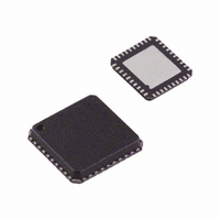
AD9948KCP Analog Devices Inc, AD9948KCP Datasheet - Page 20

AD9948KCP
Manufacturer Part Number
AD9948KCP
Description
IC CCD SIGNAL PROCESSOR 40-LFCSP
Manufacturer
Analog Devices Inc
Type
CCD Signal Processor, 10-Bitr
Datasheet
1.AD9948KCPZRL.pdf
(28 pages)
Specifications of AD9948KCP
Rohs Status
RoHS non-compliant
Input Type
Logic
Output Type
Logic
Interface
3-Wire Serial
Mounting Type
Surface Mount
Package / Case
40-LFCSP
Current - Supply
-
Available stocks
Company
Part Number
Manufacturer
Quantity
Price
Company:
Part Number:
AD9948KCP
Manufacturer:
ADI
Quantity:
210
Part Number:
AD9948KCPZ
Manufacturer:
ADI/亚德诺
Quantity:
20 000
Part Number:
AD9948KCPZRL
Manufacturer:
ADI/亚德诺
Quantity:
20 000
ANALOG FRONT END DESCRIPTION AND OPERATION
The AD9948 signal processing chain is shown in Figure 15. Each
processing step is essential in achieving a high quality image from
the raw CCD pixel data.
DC Restore
To reduce the large dc offset of the CCD output signal,
a dc restore circuit is used with an external 0.1 µF series cou-
pling capacitor. This restores the dc level of the CCD signal to
approximately 1.5 V to be compatible with the 3 V supply voltage
of the AD9948.
Correlated Double Sampler
The CDS circuit samples each CCD pixel twice to extract the
video information and reject low frequency noise. The timing
shown in Figure 5 illustrates how the two internally generated
CDS clocks, SHP and SHD, are used to sample the reference
level and the CCD signal level, respectively. The placement of
the SHP and SHD sampling edges is determined by the setting
of the SAMPCONTROL register located at Address 0x63.
Placement of these two clock signals is critical in achieving the
best performance from the CCD.
The gain in the CDS is fixed at 0 dB by default. Using Bits D10
and D11 in the AFE operation register, the gain may be reduced
to –2 dB or –4 dB. This will allow the AD9948 to accept an input
signal of greater than 1 V p-p. See Table VIII for register details.
Operation Register Bits
D11
0
0
1
1
AD9948
1.0 F
D10
0
1
0
1
Table XVI. Adjustable CDS Gain
CCDIN
DC RESTORE
0dB, –2dB, –4dB
1.5V
CDS Gain
0 dB
–2 dB
–4 dB
0 dB
SHP
CDS
SHD
SHP SHD
GENERATION
PRECISION
Figure 15. Analog Front End Functional Block Diagram
TIMING
REGISTERS
PxGA GAIN
0dB ~ 18dB
PHASE
DOUT
PxGA
Max CDS Input
1.0 V p-p
1.2 V p-p
1.6 V p-p
1.0 V p-p
CLPOB PBLK
GENERATION
TIMING
REGISTER
VGA GAIN
6dB ~ 42dB
V-H
VGA
–20–
PxGA
The PxGA provides separate gain adjustment for the individual
color pixels. A programmable gain amplifier with four separate
values, the PxGA has the capability to multiplex its gain value on
a pixel-to-pixel basis (see Figure 16). This allows lower output
color pixels to be gained up to match higher output color pixels.
Also, the PxGA may be used to adjust the colors for white bal-
ance, reducing the amount of digital processing that is needed.
The four different gain values are switched according to the color
steering circuitry. Three different color steering modes for differ-
ent types of CCD color filter arrays are programmable in the AFE
CTLMODE register at Address 0x03 (see Figures 18a to 18c for
timing examples). For example, progressive steering mode accom-
modates the popular Bayer arrangement of red, green, and blue
filters (see Figure 17a).
DAC
CDS
SHP/SHD
DIGITAL
FILTER
VD
HD
OPTICAL BLACK
INTERNAL
CLAMP
Figure 16. PxGA Block Diagram
PxGA
8
1.0V
10-BIT
1.0 F 1.0 F
REFB
V
ADC
REF
2V FULL SCALE
STEERING
CONTROL
2.0V
REFT
COLOR
2
MUX
CLAMP LEVEL
4:1
REGISTER
VGA
8
CLPOB
3
GAIN0
GAIN1
GAIN2
GAIN3
OUTPUT
AD9948
LATCH
DATA
PBLK
PxGA STEERING
SELECTION
PxGA GAIN
REGISTERS
MODE
PHASE
DOUT
10
DOUT
CONTROL
REGISTER
BITS D0–D1
REV. 0


