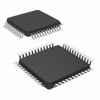
DS90UR241IVS/NOPB National Semiconductor, DS90UR241IVS/NOPB Datasheet - Page 14

DS90UR241IVS/NOPB
Manufacturer Part Number
DS90UR241IVS/NOPB
Description
IC SER/DESER 5-43MHZ 24B 48-TQFP
Manufacturer
National Semiconductor
Datasheet
1.DS90UR241IVSNOPB.pdf
(26 pages)
Specifications of DS90UR241IVS/NOPB
Function
Serializer/Deserializer
Data Rate
1.03Gbps
Input Type
LVCMOS
Output Type
LVDS
Number Of Inputs
1
Number Of Outputs
24
Voltage - Supply
3 V ~ 3.6 V
Operating Temperature
-40°C ~ 105°C
Mounting Type
Surface Mount
Package / Case
48-TQFP, 48-VQFP
For Use With
SERDESUR-43USB - BOARD EVAL DS90UR124,DS90UR241
Lead Free Status / RoHS Status
Lead free / RoHS Compliant
Other names
*DS90UR241IVS/NOPB
DS90UR241IVSCT
DS90UR241IVSCT
DS90UR241IVSCT
DS90UR241IVSCT
Available stocks
Company
Part Number
Manufacturer
Quantity
Price
Company:
Part Number:
DS90UR241IVS/NOPB
Manufacturer:
NS
Quantity:
960
Company:
Part Number:
DS90UR241IVS/NOPB
Manufacturer:
TI
Quantity:
898
Company:
Part Number:
DS90UR241IVS/NOPB
Manufacturer:
Texas Instruments
Quantity:
10 000
www.national.com
CONTROL AND CONFIGURATION PINS
9
24
18
23
11
12
5, 8,
13
LVDS SERIAL INTERFACE PINS
20
19
POWER / GROUND PINS
22
21
16
17
14
15
30
31
7
6
42
43
Pin #
TPWDNB
VODSEL
DEN
PRE
TRFB
RAOFF
RES0
D
D
VDD
VSS
VDD
VSS
VDD
VSS
VDD
VSS
VDD
VSS
VDD
VSS
OUT+
OUT−
Pin Name
LVCMOS_I
LVCMOS_I
LVCMOS_I
LVCMOS_I
LVCMOS_I
LVCMOS_I
LVCMOS_I
LVDS_O
LVDS_O
VDD
GND
VDD
GND
VDD
GND
VDD
GND
VDD
GND
VDD
GND
I/O/PWR
Transmitter Power Down Bar
TPWDNB = H; Transmitter is Enabled and ON
TPWDNB = L; Transmitter is in power down mode (Sleep), LVDS Driver D
in TRI-STATE stand-by mode, PLL is shutdown to minimize power consumption.
VOD Level Select
VODSEL = L; LVDS Driver Output is ±500 mV (R
VODSEL = H; LVDS Driver Output is ±900 mV (R
For normal applications, set this pin LOW. For long cable applications where a larger VOD is
required, set this pin HIGH.
Transmitter Data Enable
DEN = H; LVDS Driver Outputs are Enabled (ON).
DEN = L; LVDS Driver Outputs are Disabled (OFF), Transmitter LVDS Driver D
are in TRI-STATE, PLL still operational and locked to TCLK.
Pre-emphasis Level Select
PRE = NC (No Connect); Pre-emphasis is Disabled (OFF).
Pre-emphasis is active when input is tied to VSS through external resistor R
determines pre-emphasis level. Recommended value R
R
Transmitter Clock Edge Select Pin
TRFB = H; Parallel Interface Data is strobed on the Rising Clock Edge.
TRFB = L; Parallel Interface Data is strobed on the Falling Clock Edge
Randomizer Control Input Pin
RAOFF = H, Backwards compatible mode for use with DS90C124 Deserializer.
RAOFF = L; Additional randomization ON (Default), Selects 2E7 LSFR setting.
See Table 1 for more details.
Reserved. This pin MUST be tied LOW.
Transmitter LVDS True (+) Output.
This output is intended to be loaded with a 100Ω load to the D
be AC Coupled to this pin with a 100 nF capacitor.
Transmitter LVDS Inverted (-) Output
This output is intended to be loaded with a 100Ω load to the D
be AC Coupled to this pin with a 100 nF capacitor.
Analog Voltage Supply, LVDS Output POWER
Analog Ground, LVDS Output GROUND
Analog Voltage Supply, VCO POWER
Analog Ground, VCO GROUND
Analog Voltage Supply, PLL POWER
Analog Ground, PLL GROUND
Digital Voltage Supply, Serializer POWER
Digital Ground, Serializer GROUND
Digital Voltage Supply, Serializer Logic POWER
Digital Ground, Serializer Logic GROUND
Digital Voltage Supply, Serializer INPUT POWER
Digital Ground, Serializer Input GROUND
PREmin
= 6 kΩ
14
Description
L
L
= 100Ω)
= 100Ω)
PRE
≥
OUT+
OUT-
6 kΩ; I
pin. The interconnect should
pin. The interconnect should
max
= [48 / R
OUT
PRE
(+/-) Outputs are
OUT
. Resistor value
PRE
(+/-) Outputs
],


