DS90UR241IVS/NOPB National Semiconductor, DS90UR241IVS/NOPB Datasheet - Page 18
DS90UR241IVS/NOPB
Manufacturer Part Number
DS90UR241IVS/NOPB
Description
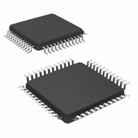
IC SER/DESER 5-43MHZ 24B 48-TQFP
Manufacturer
National Semiconductor
Datasheet
1.DS90UR241IVSNOPB.pdf
(26 pages)
Specifications of DS90UR241IVS/NOPB
Function
Serializer/Deserializer
Data Rate
1.03Gbps
Input Type
LVCMOS
Output Type
LVDS
Number Of Inputs
1
Number Of Outputs
24
Voltage - Supply
3 V ~ 3.6 V
Operating Temperature
-40°C ~ 105°C
Mounting Type
Surface Mount
Package / Case
48-TQFP, 48-VQFP
For Use With
SERDESUR-43USB - BOARD EVAL DS90UR124,DS90UR241
Lead Free Status / RoHS Status
Lead free / RoHS Compliant
Other names
*DS90UR241IVS/NOPB
DS90UR241IVSCT
DS90UR241IVSCT
DS90UR241IVSCT
DS90UR241IVSCT
Available stocks
Company
Part Number
Manufacturer
Quantity
Price
Company:

Part Number:
DS90UR241IVS/NOPB
Manufacturer:
NS
Quantity:
960
Company:
Part Number:
DS90UR241IVS/NOPB
Manufacturer:
TI
Quantity:
898
Company:
Part Number:
DS90UR241IVS/NOPB
Manufacturer:
Texas Instruments
Quantity:
10 000


www.national.com
RESYNCHRONIZATION
If the Deserializer loses lock, it will automatically try to re-es-
tablish lock. For example, if the embedded clock edge is not
detected one time in succession, the PLL loses lock and the
LOCK pin is driven low. The Deserializer then enters the op-
erating mode where it tries to lock to a random data stream.
It looks for the embedded clock edge, identifies it and then
proceeds through the locking process.
The logic state of the LOCK signal indicates whether the data
on ROUT is valid; when it is high, the data is valid. The system
may monitor the LOCK pin to determine whether data on the
ROUT is valid.
POWERDOWN
The Powerdown state is a low power sleep mode that the Se-
rializer and Deserializer may use to reduce power when no
data is being transferred. The TPWDNB and RPWDNB are
used to set each device into power down mode, which re-
duces supply current to the µA range. The Serializer enters
powerdown when the TPWDNB pin is driven low. In power-
down, the PLL stops and the outputs go into TRI-STATE,
disabling load current and reducing current supply. To exit
Powerdown, TPWDNB must be driven high. When the Seri-
alizer exits Powerdown, its PLL must lock to TCLK before it
is ready for the Initialization state. The system must then allow
time for Initialization before data transfer can begin. The De-
serializer enters powerdown mode when RPWDNB is driven
low. In powerdown mode, the PLL stops and the outputs enter
TRI-STATE. To bring the Deserializer block out of the pow-
erdown state, the system drives RPWDNB high.
Both the Serializer and Deserializer must reinitialize and re-
lock before data can be transferred. The Deserializer will
initialize and assert LOCK high when it is locked to the em-
bedded clock.
TRI-STATE
For the Serializer, TRI-STATE is entered when the DEN or
TPWDNB pin is driven low. This will TRI-STATE both driver
output pins (DOUT+ and DOUT−). When DEN is driven high,
the serializer will return to the previous state as long as all
other control pins remain static (TPWDNB, TRFB).
When you drive the REN or RPWDNB pin low, the Deserial-
izer enters TRI-STATE. Consequently, the receiver output
pins (ROUT0–ROUT23) and RCLK will enter TRI-STATE.
The LOCK output remains active, reflecting the state of the
PLL. The Deserializer input pins are high impedance during
receiver powerdown (RPWDNB low) and power-off (V
0V).
PRE-EMPHASIS
The DS90UR241 features a Pre-Emphasis function used to
compensate for long or lossy transmission media. Cable drive
is enhanced with a user selectable Pre-Emphasis feature that
provides additional output current during transitions to coun-
teract cable loading effects. The transmission distance will be
limited by the loss characteristics and quality of the media.
Pre-Emphasis adds extra current during LVDS logic transition
to reduce the cable loading effects and increase driving dis-
tance. In addition, Pre-Emphasis helps provide faster transi-
tions, increased eye openings, and improved signal integrity.
The ability of the DS90UR241 to use the Pre-Emphasis fea-
ture will extend the transmission distance up to 10 meters in
most cases.
To enable the Pre-Emphasis function, the “PRE” pin requires
one external resistor (Rpre) to Vss in order to set the addi-
tional current level. Values of Rpre should be between 6kΩ
DD
=
18
and 100MΩ. Values less than 6kΩ should not be used. A low-
er input resistor value on the ”PRE” pin increases the magni-
tude of dynamic current during data transition. The additional
source current is based on the following formula: PRE =
(R
15kΩ , then the Pre-Emphasis current is increase by an ad-
ditional 3.2 mA.
The amount of Pre-Emphasis for a given media will depend
on the transmission distance of the application. In general, too
much Pre-Emphasis can cause over or undershoot at the re-
ceiver input pins. This can result in excessive noise, crosstalk
and increased power dissipation. For short cables or dis-
tances, Pre-Emphasis may not be required. Signal quality
measurements are recommended to determine the proper
amount of Pre-Emphasis for each application.
AC-COUPLING AND TERMINATION
The DS90UR241 and DS90UR124 supports AC-coupled in-
terconnects through integrated DC balanced encoding/de-
coding scheme. To use the Serializer and Deserializer in an
AC coupled application, insert external AC coupling capaci-
tors in series in the LVDS signal path as illustrated in
20. The Deserializer input stage is designed for AC-coupling
by providing a built-in AC bias network which sets the internal
V
ac-coupling path to the signal input.
For the high-speed LVDS transmissions, the smallest avail-
able package should be used for the AC coupling capacitor.
This will help minimize degradation of signal quality due to
package parasitics. The most common used capacitor value
for the interface is 100 nF (0.1 uF) capacitor. NPO class 1 or
X7R class 2 type capacitors are recommended. 50 WVDC
should be the minimum used for the best system-level ESD
performance.
A termination resistor across DOUT± and RIN± is also re-
quired for proper operation to be obtained. The termination
resistor should be equal to the differential impedance of the
media being driven. This should be in the range of 90 to 132
Ohms. 100 Ohms is a typical value common used with stan-
dard 100 Ohm transmission media. This resistor is required
for control of reflections and also completes the current loop.
It should be placed as close to the Serializer DOUT± outputs
and Deserializer RIN± inputs to minimize the stub length from
the pins. To match with the deferential impedance on the
transmission line, the LVDS I/O are terminated with 100 Ohm
resistors on Serializer DOUT± outputs pins and Deserializer
RIN± input pins.
Receiver Termination Option 1
A single 100 Ohm termination resistor is placed across the
RIN± pins (see
tion at the Receiver inputs. Other options may be used to
increase noise tolerance.
Receiver Termination Option 2
For additional EMI tolerance, two 50 Ohm resistors may be
used in place of the single 100 Ohm resistor. A small capacitor
is tied from the center point of the 50 Ohm resistors to ground
(see
impedance path for noise suppression. Value is not critical,
4.7nF maybe used with general applications.
Receiver Termination Option 3
For high noise environments an additional voltage divider
network may be connected to the center point. This has the
advantage of a providing a DC low-impedance path for noise
suppression. Use resistor values in the range of 100Ω-2KΩ
CM
PRE
to +1.8V. With AC signal coupling, capacitors provide the
Figure
≥
6kΩ); I
22). This provides a high-frequency low
Figure
MAX
= [48 / R
20). This provides the signal termina-
PRE
]. For example if Rpre =
Figure
Related parts for DS90UR241IVS/NOPB
Image
Part Number
Description
Manufacturer
Datasheet
Request
R

Part Number:
Description:
National Semiconductor [8-Bit D/A Converter]
Manufacturer:
National Semiconductor
Datasheet:
Part Number:
Description:
National Semiconductor [Media Coprocessor]
Manufacturer:
National Semiconductor
Datasheet:
Part Number:
Description:
Digitally Controlled Tone and Volume Circuit with Stereo Audio Power Amplifier, Microphone Preamp Stage and National 3D Sound
Manufacturer:
National Semiconductor
Datasheet:
Part Number:
Description:
Digitally Controlled Tone and Volume Circuit with Stereo Audio Power Amplifier, Microphone Preamp Stage and National 3D Sound
Manufacturer:
National Semiconductor
Datasheet:
Part Number:
Description:
AC97 Rev 2 Codec with Sample Rate Conversion and National 3D Sound
Manufacturer:
National Semiconductor
Part Number:
Description:
Manufacturer:
National Semiconductor
Datasheet:
Part Number:
Description:
Manufacturer:
National Semiconductor
Datasheet:
Part Number:
Description:
General Purpose, Low Voltage, Low Power, Rail-to-Rail Output Operational Amplifiers
Manufacturer:
National Semiconductor
Datasheet:
Part Number:
Description:
8-bit 20 MSPS flash A/D converter.
Manufacturer:
National Semiconductor
Datasheet:
Part Number:
Description:
Low Noise Quad Operational Amplifier
Manufacturer:
National Semiconductor
Datasheet:
Part Number:
Description:
Quad Differential Line Receivers
Manufacturer:
National Semiconductor
Datasheet:
Part Number:
Description:
Quad High Speed Trapezoidal? Bus Transceiver
Manufacturer:
National Semiconductor
Datasheet:
Part Number:
Description:
Dual Line Receiver
Manufacturer:
National Semiconductor
Datasheet:
Part Number:
Description:
TTL to 10k ECL Level Translator with Latch
Manufacturer:
National Semiconductor
Datasheet: