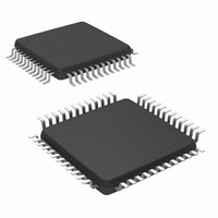
DS90UR241IVS/NOPB National Semiconductor, DS90UR241IVS/NOPB Datasheet - Page 6

DS90UR241IVS/NOPB
Manufacturer Part Number
DS90UR241IVS/NOPB
Description
IC SER/DESER 5-43MHZ 24B 48-TQFP
Manufacturer
National Semiconductor
Datasheet
1.DS90UR241IVSNOPB.pdf
(26 pages)
Specifications of DS90UR241IVS/NOPB
Function
Serializer/Deserializer
Data Rate
1.03Gbps
Input Type
LVCMOS
Output Type
LVDS
Number Of Inputs
1
Number Of Outputs
24
Voltage - Supply
3 V ~ 3.6 V
Operating Temperature
-40°C ~ 105°C
Mounting Type
Surface Mount
Package / Case
48-TQFP, 48-VQFP
For Use With
SERDESUR-43USB - BOARD EVAL DS90UR124,DS90UR241
Lead Free Status / RoHS Status
Lead free / RoHS Compliant
Other names
*DS90UR241IVS/NOPB
DS90UR241IVSCT
DS90UR241IVSCT
DS90UR241IVSCT
DS90UR241IVSCT
Available stocks
Company
Part Number
Manufacturer
Quantity
Price
Company:
Part Number:
DS90UR241IVS/NOPB
Manufacturer:
NS
Quantity:
960
Company:
Part Number:
DS90UR241IVS/NOPB
Manufacturer:
TI
Quantity:
898
Company:
Part Number:
DS90UR241IVS/NOPB
Manufacturer:
Texas Instruments
Quantity:
10 000
www.national.com
t
t
t
t
t
t
t
t
t
t
t
t
t
t
t
t
t
t
RxIN_TOL-L
RxIN_TOL-R Receiver INput TOLerance
ROS
ROH
ROS
ROH
ROS
ROH
ROS
ROH
ROS
ROH
ROS
ROH
HZR
LZR
ZHR
ZLR
DD
DSR
Note 1: “Absolute Maximum Ratings” indicate limits beyond which damage to the device may occur, including inoperability and degradation of device reliability
and/or performance. Functional operation of the device and/or non-degradation at the Absolute Maximum Ratings or other conditions beyond those indicated in
the Recommended Operating Conditions is not implied. The Recommended Operating Conditions indicate conditions at which the device is functional and the
device should not be operated beyond such conditions.
Note 2: 4L =4 layer PCB per JEDEC specification, 2L = 2 layer PCB per JEDEC specification.
Note 3: The Electrical Characteristics tables list guaranteed specifications under the listed Recommended Operating Conditions except as otherwise modified
or specified by the Electrical Characteristics Conditions and/or Notes. Typical specifications are estimations only and are not guaranteed.
Note 4: Typical values represent most likely parametric norms at V
product characterization and are not guaranteed.
Note 5: Current into device pins is defined as positive. Current out of a device pin is defined as negative. Voltages are referenced to ground except VOD, ΔVOD,
VTH and VTL which are differential voltages.
Note 6: When the Serializer output is at TRI-STATE the Deserializer will lose PLL lock. Resynchronization MUST occur before data transfer.
Note 7: t
Note 8: RxIN_TOL is a measure of how much phase noise (jitter) the Deserializer can tolerate in the incoming data stream before bit errors occur. It is a
measurement in reference with the ideal bit position, please see National’s AN-1217 for detail.
Note 9: Specification is guaranteed by characterization and is not tested in production.
Note 10: t
Symbol
DSR
JIT
is the time required by the Deserializer to obtain lock when exiting powerdown mode.
(@BER of 10e-9) specifies the allowable jitter on TCLK. t
R
RCLK (Group 1)
R
(Group 1)
R
RCLK (Group 2)
R
RCLK (Group 2)
R
RCLK (Group 3)
R
RCLK (Group 3)
R
RCLK (Group 1)
R
(Group 1)
R
RCLK (Group 2)
R
RCLK (Group 2)
R
RCLK (Group 3)
R
RCLK (Group 3)
HIGH to TRI-STATE Delay
LOW to TRI-STATE Delay
TRI-STATE to HIGH Delay
TRI-STATE to LOW Delay
Deserializer Delay
Deserializer PLL Lock Time
from Powerdown
Receiver INput TOLerance
Left
Right
OUT
OUT
OUT
OUT
OUT
OUT
OUT
OUT
OUT
OUT
OUT
OUT
(0:7) Setup Data to
(0:7) Hold Data to RCLK
(8:15) Setup Data to
(8:15) Hold Data to
(16:23) Setup Data to
(16:23) Setup Data to
(0:7) Setup Data to
(0:7) Hold Data to RCLK
(8:15) Setup Data to
(8:15) Hold Data to
(16:23) Setup Data to
(16:23) Setup Data to
Parameter
PTOSEL = L,
SLEW = H,
(Figure
PTOSEL = L,
SLEW = H,
(Figure
PTOSEL = H,
SLEW = H,
(Figure
PTOSEL = H,
(Figure
PTOSEL = H,
(Figure
(Note
(Note
(Note
(Figure
(Note 8),(Note
Note
(Figure
Conditions
11)
7,
8,
11)
16)
16)
15)
14)
12)
17)
17)
Note
Note
DD
= 3.3V, Ta = +25 degC, and at the Recommended Operation Conditions at the time of
JIT
9)
9),
not included in TxOUT_E_O parameter.
9,
R
R
LOCK
R
R
R
LOCK
R
R
RCLK, LOCK
RCLK
5 MHz
43 MHz
5 MHz–43 MHz
5 MHz–43 MHz
6
OUT
OUT
OUT
OUT
OUT
OUT
OUT
Pin/Freq.
[0:7]
[0:7]
[8:15],
[16:23]
[8:15],
[16:23]
[0:23],
(0.35)*
(0.35)*
(0.35)*
(0.35)*
(0.35)*
(0.35)*
(0.35)*
(0.35)*
(0.35)*
(0.35)*
(0.35)*
(0.35)*
t
t
t
t
t
t
t
t
t
t
t
t
Min
RCP
RCP
RCP
RCP
RCP
RCP
RCP
RCP
RCP
RCP
RCP
RCP
[5+(5/56)]T+3.7
(0.5*t
(0.5*t
(0.5*t
(0.5*t
(0.5*t
(0.5*t
(0.5*t
(0.5*t
(0.5*t
(0.5*t
(0.5*t
(0.5*t
RCP
RCP
RCP
RCP
RCP
RCP
RCP
RCP
RCP
RCP
RCP
RCP
Typ
3
3
3
3
)–3 UI
)–3 UI
)–3 UI
)–3 UI
)–3 UI
)–3 UI
)–2 UI
)+2 UI
)−1 UI
)+1 UI
)+1 UI
)–1 UI
[5+(5/56)]T
128k*T
128k*T
Max
0.25
0.25
10
10
10
10
+8
Units
ms
ms
ns
ns
ns
ns
ns
ns
ns
ns
ns
ns
ns
ns
ns
ns
ns
ns
ns
UI
UI


