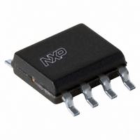
PCA9517AD,112 NXP Semiconductors, PCA9517AD,112 Datasheet - Page 10

PCA9517AD,112
Manufacturer Part Number
PCA9517AD,112
Description
IC I2C BUS REPEATER 8-SOIC
Manufacturer
NXP Semiconductors
Type
Repeaterr
Datasheet
1.PCA9517AD112.pdf
(19 pages)
Specifications of PCA9517AD,112
Tx/rx Type
I²C Logic
Delay Time
170ns
Capacitance - Input
6pF
Voltage - Supply
2.7 V ~ 5.5 V
Current - Supply
5mA
Mounting Type
Surface Mount
Package / Case
8-SOIC (3.9mm Width)
Lead Free Status / RoHS Status
Lead free / RoHS Compliant
Other names
935285763112
PCA9517AD
PCA9517AD
PCA9517AD
PCA9517AD
Available stocks
Company
Part Number
Manufacturer
Quantity
Price
Company:
Part Number:
PCA9517AD,112
Manufacturer:
NXP
Quantity:
12 000
NXP Semiconductors
Table 5.
V
[1]
[2]
[3]
10. Dynamic characteristics
Table 6.
V
[1]
[2]
[3]
[4]
[5]
[6]
[7]
PCA9517A_2
Product data sheet
Symbol
Enable
V
V
I
I
C
Symbol
t
t
t
t
t
t
t
t
t
t
IL(EN)
LI
PLH
PHL
TLH
THL
PLH
PHL
TLH
THL
su
h
CC
CC
IL
IH
i
= 2.7 V to 5.5 V; GND = 0 V; T
LOW-level supply voltage.
V
SDAB/SCLB lines.
V
= 2.7 V to 5.5 V; GND = 0 V; T
Times are specified with loads of 1.35 k pull-up resistance and 57 pF load capacitance on port B, and 167
57 pF load capacitance on port A. Different load resistance and capacitance will alter the RC time constant, thereby changing the
propagation delay and transition times.
Pull-up voltages are V
Typical values were measured with V
The t
on port A if V
Typical value measured with V
The proportional delay data from port A to port B is measured at 0.3V
The enable pin, EN, should only change state when the global bus and the repeater port are in an idle state.
IL
IL
specification is for the first LOW level seen by the SDAB/SCLB lines. V
for port A with envelope noise must be below 0.3V
PLH
Parameter
LOW-to-HIGH propagation delay
HIGH-to-LOW propagation delay
LOW to HIGH output transition time
HIGH to LOW output transition time
LOW-to-HIGH propagation delay
HIGH-to-LOW propagation delay
LOW to HIGH output transition time
HIGH to LOW output transition time
set-up time
hold time
Static characteristics
Dynamic characteristics
delay data from port B to port A is measured at 0.5 V on port B to 0.5V
Parameter
LOW-level input voltage
HIGH-level input voltage
LOW-level input current on
pin EN
input leakage current
input capacitance
CC(A)
is greater than 2 V.
CC(A)
on port A and V
CC(A)
amb
amb
…continued
= 2.7 V at T
CC(A)
= 40 C to +85 C; unless otherwise specified.
= 40 C to +85 C; unless otherwise specified.
= 3.3 V at T
CC(B)
amb
on port B.
Conditions
V
V
I
I
= 25 C.
= 0.2 V, EN; V
= 3.0 V or 0 V
Conditions
port B to port A;
port B to port A;
port A;
port A;
port A to port B;
port A to port B;
port B;
port B;
EN HIGH before START condition
EN HIGH after STOP condition
Rev. 02 — 5 May 2008
CC(A)
amb
V
V
V
V
CC(A)
CC(A)
CC(A)
CC(A)
= 25 C, unless otherwise noted.
for stable performance.
Figure 10
Figure 10
Figure 11
Figure 11
2.7 V
3 V
2.7 V
3 V
CC
CC(A)
Figure 12
Figure 10
Figure 11
Figure 11
= 3.6 V
ILc
on port A to 1.5 V on port B.
is for the second and subsequent LOW levels seen by the
CC(A)
on port A when V
Level translating I
Min
0.7V
-
-
[1][2]
0.5
1
[4]
[5]
[5]
[6]
[6]
[7]
[7]
CC(B)
Min
100
30
10
10
1
20
25
60
120
30
100
100
CC(A)
Typ
-
-
-
6
10
PCA9517A
is less than 2 V, and 1.5 V
Typ
170
80
66
20
77
70
53
79
140
48
-
-
pull-up resistance and
© NXP B.V. 2008. All rights reserved.
[3]
Max
+0.3V
5.5
+1
7
2
30
C-bus repeater
Max
250
110
300
30
105
175
110
230
170
90
-
-
CC(B)
10 of 19
Unit
V
V
pF
Unit
ns
ns
ns
ns
ns
ns
ns
ns
ns
ns
ns
ns
A
A


