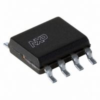
PCA9508D,118 NXP Semiconductors, PCA9508D,118 Datasheet - Page 4

PCA9508D,118
Manufacturer Part Number
PCA9508D,118
Description
IC I2C/SMBUS BIDIR-REPEAT 8SOIC
Manufacturer
NXP Semiconductors
Type
Repeaterr
Datasheet
1.PCA9508D112.pdf
(21 pages)
Specifications of PCA9508D,118
Package / Case
8-SOIC (3.9mm Width)
Tx/rx Type
I²C Logic
Delay Time
170ns
Capacitance - Input
5.2pF
Voltage - Supply
2.7 V ~ 5.5 V
Current - Supply
170mA
Mounting Type
Surface Mount
Logic Family
SDA, SCL
Propagation Delay Time
170 ns
Operating Supply Voltage
0.9 V to 5.5 V
Power Dissipation
100 mW
Operating Temperature Range
- 40 C to + 85 C
Logic Type
I2C Bus
Mounting Style
SMD/SMT
Output Voltage
0.52 V
Function
I2C Bus Repeater
Operating Temperature (max)
85C
Operating Temperature (min)
-40C
Package Type
SO
Pin Count
8
Mounting
Surface Mount
Lead Free Status / RoHS Status
Lead free / RoHS Compliant
Lead Free Status / RoHS Status
Lead free / RoHS Compliant, Lead free / RoHS Compliant
Other names
935285665118
PCA9508D-T
PCA9508D-T
PCA9508D-T
PCA9508D-T
NXP Semiconductors
5. Pinning information
6. Functional description
PCA9508_1
Product data sheet
5.1 Pinning
5.2 Pin description
Table 3.
Refer to
The PCA9508 enables I
without degradation of system performance. The PCA9508 contains two bidirectional
open-drain buffers specifically designed to provide superior hot-swap and/or support
up-translation/down-translation between the low voltage (as low as 0.9 V) and a 3.3 V or
5 V I
device is unpowered (V
circuit that keeps the output drivers turned off until V
above 0.8 V. V
used to provide the 0.5V
good detect circuit. The PCA9508 logic and all I/Os are powered by the V
An undervoltage/initialization circuit holds the PCA9508 in a disconnected state which
presents high-impedance to all SDA and SCL pins during power-up. A LOW on the enable
pin (EN) also forces the parts into the disconnected state. As the power supply is brought
up and EN is HIGH or the part is powered and EN is taken from LOW to HIGH it enters an
initialization state where the internal references are stabilized. At the end of the
initialization state the ‘STOP bit and bus idle’ detect circuit is enabled. With the EN pin
Symbol
V
SCLA
SDAA
GND
EN
SDAB
SCLB
V
Fig 2.
CC(A)
CC(B)
2
C-bus or SMBus. All inputs and I/Os are overvoltage tolerant to 5.5 V even when the
V
SDAA
SCLA
CC(A)
Figure 1 “Functional diagram of
GND
Pin configuration for SO8
Pin description
1
2
3
4
CC(B)
Pin
1
2
3
4
5
6
7
8
PCA9508D
and V
002aac652
Rev. 01 — 28 April 2008
CC(B)
2
CC(A)
C-bus or SMBus translation down to V
Description
A side supply voltage (0.9 V to 5.5 V)
open-drain input/output serial clock A side bus
open-drain input/output serial data A side bus
supply ground (0 V)
active HIGH repeater enable input with an internal pull-up (100 k
open-drain input/output serial data B side bus
open-drain input/output serial clock B side bus
B side supply voltage (2.7 V to 5.5 V)
CC(A)
and/or V
reference to the A side input comparators and for the power
8
7
6
5
can be applied in any sequence at power-up. V
V
SCLB
SDAB
EN
CC(B)
CC(A)
Hot swappable level translating I
PCA9508”.
= 0 V). The PCA9508 includes a power-up
Fig 3.
V
SDAA
SCLA
CC(B)
CC(A)
GND
Pin configuration for TSSOP8
is above 2.5 V and the V
1
2
3
4
PCA9508DP
CC(A)
002aac653
as low as 0.9 V
PCA9508
© NXP B.V. 2008. All rights reserved.
2
CC(B)
C-bus repeater
8
7
6
5
CC(A)
V
SCLB
SDAB
EN
pin.
CC(B)
CC(A)
is only
4 of 21
is


