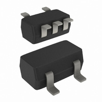
74LVC1G66GW,125 NXP Semiconductors, 74LVC1G66GW,125 Datasheet - Page 15

74LVC1G66GW,125
Manufacturer Part Number
74LVC1G66GW,125
Description
IC SWITCH SPST 5TSSOP
Manufacturer
NXP Semiconductors
Series
74LVCr
Type
Analog Switchr
Datasheet
1.74LVC1G66GM115.pdf
(25 pages)
Specifications of 74LVC1G66GW,125
Package / Case
6-TSSOP (5 lead), SC-88A, SOT-353
Function
Switch
Circuit
1 x SPST- NO
On-state Resistance
6 Ohm
Voltage Supply Source
Single Supply
Voltage - Supply, Single/dual (±)
1.65 V ~ 5.5 V
Current - Supply
0.1µA
Operating Temperature
-40°C ~ 125°C
Mounting Type
Surface Mount
Switch Configuration
SPST
On Resistance (max)
34 Ohm (Typ) @ 1.95 V
On Time (max)
5.3 ns (Typ) @ 1.95 V
Off Time (max)
4.2 ns (Typ) @ 1.95 V
Supply Voltage (max)
5.5 V
Supply Voltage (min)
1.65 V
Maximum Power Dissipation
250 mW
Maximum Operating Temperature
+ 125 C
Mounting Style
SMD/SMT
Minimum Operating Temperature
- 40 C
Switch Current (typ)
0.0001 mA @ 3.3 V
Multiplexer Configuration
Single SPST
Number Of Inputs
1
Number Of Outputs
1
Number Of Channels
1
Analog Switch On Resistance
34@1.95VOhm
Package Type
TSSOP
Power Supply Requirement
Single
Single Supply Voltage (min)
1.65V
Single Supply Voltage (typ)
3/5V
Single Supply Voltage (max)
5.5V
Dual Supply Voltage (min)
Not RequiredV
Dual Supply Voltage (typ)
Not RequiredV
Dual Supply Voltage (max)
Not RequiredV
Power Dissipation
250mW
Mounting
Surface Mount
Pin Count
5
Operating Temp Range
-40C to 125C
Operating Temperature Classification
Automotive
Lead Free Status / RoHS Status
Lead free / RoHS Compliant
Lead Free Status / RoHS Status
Lead free / RoHS Compliant, Lead free / RoHS Compliant
Other names
568-4614-2
74LVC1G66GW-G
74LVC1G66GW-G
935269058125
74LVC1G66GW-G
74LVC1G66GW-G
935269058125
NXP Semiconductors
74LVC1G66
Product data sheet
Fig 21. Test circuit for measuring isolation (OFF-state)
Fig 22. Test circuit for measuring crosstalk between digital input and switch
Fig 23. Test circuit for measuring charge injection
Adjust f
Q
ΔV
R
V
gen
gen
inj
O
= ΔV
= output voltage variation.
= generator voltage.
= generator resistance.
i
voltage to obtain 0 dBm level at input.
O
× C
L
.
G
G
input (E)
f i
logic
V
logic
input
logic
input
O
0.1 μF
50 Ω
All information provided in this document is subject to legal disclaimers.
0.5V
50 Ω
R gen
off
V gen
0.5V
CC
R L
CC
V
Rev. 7 — 30 July 2010
600 Ω
IL
Y/Z
Y/Z
Y/Z
E
E
E
V
V
CC
CC
V
CC
on
Z/Y
Z/Y
Z/Y
0.5V
CC
R L
1 MΩ
R L
C L
0.5V
001aam398
dB
C L
C L
0.1 nF
001aam395
001aam396
CC
R L
off
001aam394
ΔV
O
V
V
O
O
V
O
74LVC1G66
© NXP B.V. 2010. All rights reserved.
Bilateral switch
15 of 25


