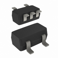
74LVC1G66GW,125 NXP Semiconductors, 74LVC1G66GW,125 Datasheet - Page 4

74LVC1G66GW,125
Manufacturer Part Number
74LVC1G66GW,125
Description
IC SWITCH SPST 5TSSOP
Manufacturer
NXP Semiconductors
Series
74LVCr
Type
Analog Switchr
Datasheet
1.74LVC1G66GM115.pdf
(25 pages)
Specifications of 74LVC1G66GW,125
Package / Case
6-TSSOP (5 lead), SC-88A, SOT-353
Function
Switch
Circuit
1 x SPST- NO
On-state Resistance
6 Ohm
Voltage Supply Source
Single Supply
Voltage - Supply, Single/dual (±)
1.65 V ~ 5.5 V
Current - Supply
0.1µA
Operating Temperature
-40°C ~ 125°C
Mounting Type
Surface Mount
Switch Configuration
SPST
On Resistance (max)
34 Ohm (Typ) @ 1.95 V
On Time (max)
5.3 ns (Typ) @ 1.95 V
Off Time (max)
4.2 ns (Typ) @ 1.95 V
Supply Voltage (max)
5.5 V
Supply Voltage (min)
1.65 V
Maximum Power Dissipation
250 mW
Maximum Operating Temperature
+ 125 C
Mounting Style
SMD/SMT
Minimum Operating Temperature
- 40 C
Switch Current (typ)
0.0001 mA @ 3.3 V
Multiplexer Configuration
Single SPST
Number Of Inputs
1
Number Of Outputs
1
Number Of Channels
1
Analog Switch On Resistance
34@1.95VOhm
Package Type
TSSOP
Power Supply Requirement
Single
Single Supply Voltage (min)
1.65V
Single Supply Voltage (typ)
3/5V
Single Supply Voltage (max)
5.5V
Dual Supply Voltage (min)
Not RequiredV
Dual Supply Voltage (typ)
Not RequiredV
Dual Supply Voltage (max)
Not RequiredV
Power Dissipation
250mW
Mounting
Surface Mount
Pin Count
5
Operating Temp Range
-40C to 125C
Operating Temperature Classification
Automotive
Lead Free Status / RoHS Status
Lead free / RoHS Compliant
Lead Free Status / RoHS Status
Lead free / RoHS Compliant, Lead free / RoHS Compliant
Other names
568-4614-2
74LVC1G66GW-G
74LVC1G66GW-G
935269058125
74LVC1G66GW-G
74LVC1G66GW-G
935269058125
NXP Semiconductors
8. Limiting values
Table 5.
In accordance with the Absolute Maximum Rating System (IEC 60134). Voltages are referenced to GND (ground = 0 V).
[1]
[2]
[3]
9. Recommended operating conditions
Table 6.
[1]
[2]
74LVC1G66
Product data sheet
Symbol
V
V
I
I
V
I
I
I
T
P
Symbol
V
V
V
T
Δt/ΔV
IK
SK
SW
CC
GND
stg
amb
CC
I
SW
tot
CC
I
SW
The minimum input voltage rating may be exceeded if the input current rating is observed.
The minimum and maximum switch voltage ratings may be exceeded if the switch clamping current rating is observed.
For TSSOP5 and SC-74A packages: above 87.5 °C the value of P
For XSON6 packages: above 118 °C the value of P
To avoid sinking GND current from terminal Z when switch current flows in terminal Y, the voltage drop across the bidirectional switch
must not exceed 0.4 V. If the switch current flows into terminal Z, no GND current will flow from terminal Y. In this case, there is no limit
for the voltage drop across the switch.
Applies to control signal levels.
Limiting values
Recommended operating conditions
Parameter
supply voltage
input voltage
switch voltage
ambient temperature
input transition rise and
fall rate
Parameter
supply voltage
input voltage
input clamping current
switch clamping current
switch voltage
switch current
supply current
ground current
storage temperature
total power dissipation
All information provided in this document is subject to legal disclaimers.
Conditions
V
V
Conditions
V
V
enable and disable mode
V
T
CC
CC
amb
I
I
SW
< −0.5 V or V
< −0.5 V or V
tot
= 1.65 V to 2.7 V
= 2.7 V to 5.5 V
> −0.5 V or V
= −40 ° C to +125 °C
Rev. 7 — 30 July 2010
derates linearly with 7.8 mW/K.
I
I
> V
> V
tot
SW
derates linearly with 4.0 mW/K.
CC
CC
< V
+ 0.5 V
+ 0.5 V
CC
+ 0.5 V
[1]
[2]
[2]
Min
1.65
0
0
−40
-
-
[1]
[2]
[3]
-
Min
−0.5
−0.5
−50
-
−0.5
-
−100
−65
-
Typ
-
-
-
-
-
-
74LVC1G66
Max
+6.5
+6.5
-
±50
±50
100
-
+150
250
V
CC
© NXP B.V. 2010. All rights reserved.
+ 0.5
Max
5.5
5.5
V
+125
20
10
Bilateral switch
CC
Unit
V
V
mA
mA
V
mA
mA
mA
°C
mW
Unit
V
V
V
°C
ns/V
ns/V
4 of 25


