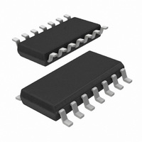
74LV4066D,112 NXP Semiconductors, 74LV4066D,112 Datasheet - Page 14

74LV4066D,112
Manufacturer Part Number
74LV4066D,112
Description
IC SWITCH QUAD 1X2 14SOIC
Manufacturer
NXP Semiconductors
Series
74LVr
Type
Analog Switchr
Datasheet
1.74LV4066DB112.pdf
(23 pages)
Specifications of 74LV4066D,112
Function
Switch
Circuit
4 x 1:2
Voltage Supply Source
Dual Supply
Voltage - Supply, Single/dual (±)
±1 V ~ 6 V
Current - Supply
40µA
Operating Temperature
-40°C ~ 125°C
Mounting Type
Surface Mount
Package / Case
14-SOIC (0.154", 3.90mm Width)
Package
14SO
Maximum On Resistance
130@2V Ohm
Maximum Propagation Delay Bus To Bus
8(Typ)@1.2V|5(Typ)@2V|3(Typ)@3.6V|2@4.5V|2(Typ)|(Typ)|(Typ)|(Typ)@6V ns
Maximum Low Level Output Current
25 mA
Maximum Turn-off Time
50(Typ)@1.2V ns
Maximum Turn-on Time
40(Typ)@1.2V ns
Switch Architecture
SPST
Power Supply Type
Single
Lead Free Status / RoHS Status
Lead free / RoHS Compliant
Other names
568-4600-5
74LV4066D
74LV4066D
935088370112
74LV4066D
74LV4066D
935088370112
Philips Semiconductors
13. Additional dynamic characteristics
9397 750 15209
Product data sheet
Table 12:
Voltages are referenced to GND (ground = 0 V); V
assigned as an input; V
[1]
[2]
[3]
Symbol
d
V
f
C
max
sin
OFF(feedthru)
ct(S)
ct(pp)
S
Adjust input voltage V
Pin nE: square wave between V
Adjust input voltage V
Additional dynamic characteristics
Parameter
sine-wave distortion
switch OFF-state
signal feed-through
attenuation
crosstalk between
switches
crosstalk voltage
between enable input
to any switch
(peak-to-peak value)
minimum frequency
response ( 3 dB)
maximum switch
capacitance
os
is
is
is 0 dBm level (0 dBm = 1 mW into 600 ).
is 0 dBm level at V
is the output voltage at pin nY or nZ, whichever is assigned as an output.
Rev. 03 — 4 July 2005
CC
and GND, t
Conditions
R
C
R
C
R
C
Figure 14
R
C
R
C
Figure 17
R
see
L
L
L
L
L
L
L
L
L
L
L
V
V
V
V
V
V
V
V
V
V
V
V
= 10 k ; f = 1 kHz;
= 50 pF; see
= 10 k ; f = 10 kHz;
= 50 pF; see
= 600 k ; f = 1 MHz;
= 50 pF; see
= 600 k ; f = 1 MHz;
= 50 pF; see
= 600 k ; f = 1 MHz;
= 50 pF; see
= 50 k ; C
CC
CC
CC
CC
CC
CC
CC
CC
CC
CC
CC
CC
os
Figure 18
for 1 MHz (0 dBm = 1 mW into 50 ).
= 3.0 V; V
= 6.0 V; V
= 3.0 V; V
= 6.0 V; V
= 3.0 V
= 6.0 V
= 3.0 V
= 6.0 V
= 3.0 V
= 6.0 V
= 3.0 V
= 6.0 V
r
= t
f
is
= 6 ns.
is the input voltage at pin nY or nZ, whichever is
L
and
= 50 pF;
Figure 12
Figure 12
Figure 13
Figure 15
Figure 16
is
is
is
is
= 2.75 V (p-p)
= 5.50 V (p-p)
= 2.75 V (p-p)
= 5.50 V (p-p)
Figure 19
© Koninklijke Philips Electronics N.V. 2005. All rights reserved.
and
and
Quad bilateral switches
[1]
[1]
[2]
[3]
Min Typ Max Unit
-
-
-
-
-
-
-
-
-
-
-
-
-
74LV4066
0.04 -
0.02 -
0.12 -
0.06 -
110 -
220 -
180 -
200 -
8
50 -
50 -
60 -
60 -
-
14 of 23
%
%
%
%
dB
dB
dB
dB
mV
mV
MHz
MHz
pF


