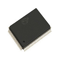
CY7C1381C-100AI Cypress Semiconductor Corp, CY7C1381C-100AI Datasheet - Page 8

CY7C1381C-100AI
Manufacturer Part Number
CY7C1381C-100AI
Description
Manufacturer
Cypress Semiconductor Corp
Datasheet
1.CY7C1381C-100AI.pdf
(36 pages)
Specifications of CY7C1381C-100AI
Density
18Mb
Access Time (max)
8.5ns
Sync/async
Synchronous
Architecture
SDR
Clock Freq (max)
100MHz
Operating Supply Voltage (typ)
3.3V
Address Bus
19b
Package Type
TQFP
Operating Temp Range
-40C to 85C
Number Of Ports
1
Supply Current
175mA
Operating Supply Voltage (min)
3.135V
Operating Supply Voltage (max)
3.6V
Operating Temperature Classification
Industrial
Mounting
Surface Mount
Pin Count
100
Word Size
36b
Number Of Words
512K
Lead Free Status / Rohs Status
Not Compliant
Document #: 38-05238 Rev. *B
CY7C1381C–Pin Definitions
V
V
V
TDO
TDI
TMS
TCK
NC
V
DDQ
SS
SSQ
SS
Name
/DNU
54,61,70,77
17,40,67,90
55,60,71,76
16,38,39,66
4,11,20,27,
5,10,21,26,
Enable)
(3-Chip
TQFP
14
-
-
-
-
H2,D3,E3,F3,H3
A1,F1,J1,M1,U1
A7,F7,J7,M7,U7
P3,D5,E5,F5,H5
B1,C1,R1,T1,T2
,J3,D4,L4,J5,R5
,T6,U6,B7,C7,R
M5,N5,P5
Enable)
(1-Chip
M3,N3,
BGA
(continued)
,K3,
,K5,
U5
U3
U2
U4
7
-
-
,
J6,J7,K5,K6,K7,
L5,L6,L7,M5,M6
B11,C2,C10,H1,
H10,N2,N5,N7,
N10,P1,P2,R2
A1,A11,B1,
L9,M3,M9,
G6,G7,H5,
,M7,N4,N8
C3,C9,D3,
C4,C5,C6,
C7,C8,D5,
D6,D7,E5,
D9,E3,E9,
F3,F9,G3,
E6,E7,F5,
F6,F7,G5,
H6,H7,J5,
K3,K9,L3,
G9,J3,J9,
Enable)
(3-Chip
H3,H9,
N3,N9
fBGA
P7
P5
R5
R7
-
-
Synchronous
Synchronous
Synchronous
Ground/DNU This pin can be connected to Ground or
JTAG-Clock
JTAG serial
JTAG serial
JTAG serial
I/O Ground
I/O Power
Ground
Supply
output
input
input
I/O
-
Power supply for the I/O circuitry.
Ground for the core of the device.
Ground for the I/O circuitry.
Serial data-out to the JTAG circuit.
Delivers data on the negative edge of TCK.
If the JTAG feature is not being utilized, this
pin should be left unconnected. This pin is
not available on TQFP packages.
Serial data-In to the JTAG circuit. Sampled
on the rising edge of TCK. If the JTAG feature
is not being utilized, this pin can be left
floating or connected to V
up resistor. This pin is not available on TQFP
packages.
Serial data-In to the JTAG circuit. Sampled
on the rising edge of TCK. If the JTAG feature
is not being utilized, this pin can be discon-
nected or connected to V
available on TQFP packages.
Clock input to the JTAG circuitry. If the
JTAG feature is not being utilized, this pin
must be connected to V
available on TQFP packages.
No Connects. Not internally connected to
the die. 18M, 36M, 72M, 144M and 288M are
address expansion pins are not internally
connected to the die.
should be left floating.
Description
SS
CY7C1381C
CY7C1383C
DD
DD
. This pin is not
. This pin is not
through a pull
Page 8 of 36
[+] Feedback


