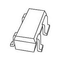
BF904WR NXP Semiconductors, BF904WR Datasheet - Page 6

BF904WR
Manufacturer Part Number
BF904WR
Description
Enhancement type Field-Effect Transistor in a plastic SOT343R package
Manufacturer
NXP Semiconductors
Datasheet
1.BF904WR.pdf
(14 pages)
Specifications of BF904WR
Application
VHF/UHF
Channel Type
N
Channel Mode
Enhancement
Continuous Drain Current
0.03A
Drain Source Voltage (max)
7V
Noise Figure (max)
2.8dB
Frequency (max)
1GHz
Package Type
CMPAK
Pin Count
3 +Tab
Input Capacitance (typ)@vds
2.2@5V@Gate 1/1.5@5V@Gate 2pF
Output Capacitance (typ)@vds
1.3@5VpF
Reverse Capacitance (typ)
0.025@5VpF
Operating Temp Range
-65C to 150C
Mounting
Surface Mount
Number Of Elements
2
Power Dissipation (max)
280mW
Screening Level
Military
Lead Free Status / Rohs Status
Compliant
Available stocks
Company
Part Number
Manufacturer
Quantity
Price
Company:
Part Number:
BF904WR
Manufacturer:
NXP
Quantity:
51 000
NXP Semiconductors
2010 Sep 15
handbook, halfpage
handbook, halfpage
N-channel dual-gate MOS-FET
V
T
V
T
G2-S
j
DS
j
(mS)
(mA)
= 25 C.
y fs
= 25 C.
I D
Fig.9
= 5 V.
Fig.7 Output characteristics; typical values.
20
16
12
40
30
20
10
= 4 V.
8
4
0
0
0
0
Forward transfer admittance as a
function of drain current; typical values.
2
4
4
8
V
G1 S
1.3 V
1.2 V
1.0 V
1.1 V
0.9 V
= 1.4 V
12
6
V
G2 S
16
8
V
I
D
DS
2 V
3.5 V
3 V
2.5 V
= 4 V
MLD269
MLD272
(mA)
(V)
10
20
6
handbook, halfpage
handbook, halfpage
V
T
V
T
Fig.10 Drain current as a function of gate 1 current;
j
j
DS
DS
(mA)
(μA)
= 25 C.
= 25 C.
I G1
I D
150
100
= 5 V.
= 5 V; V
Fig.8
50
16
12
0
8
4
0
0
0
typical values.
G2-S
Gate 1 current as a function of gate 1
voltage; typical values.
= 4 V.
0.5
10
1.0
20
1.5
30
V
G2 S
Product specification
2.0
BF904WR
40
= 4 V
V
3.5 V
3 V
2.5 V
2 V
G1 S
I
G1
MLD271
MLD273
(μA)
(V)
2.5
50


