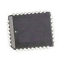
M50FW040K1 STMicroelectronics, M50FW040K1 Datasheet - Page 13

M50FW040K1
Manufacturer Part Number
M50FW040K1
Description
Flash 3.6V 4M (512Kx8)
Manufacturer
STMicroelectronics
Datasheet
1.M50FW040K1.pdf
(41 pages)
Specifications of M50FW040K1
Data Bus Width
8 bit
Memory Type
NOR
Memory Size
4 Mbit
Architecture
Sectored
Interface Type
Firmware Hub
Access Time
11 ns, 50 ns
Supply Voltage (max)
3.6 V
Supply Voltage (min)
3 V
Maximum Operating Current
20 mA
Operating Temperature
+ 70 C
Mounting Style
SMD/SMT
Package / Case
PLCC-32
Organization
512 KB x 8
Lead Free Status / Rohs Status
No
Available stocks
Company
Part Number
Manufacturer
Quantity
Price
Company:
Part Number:
M50FW040K1
Manufacturer:
ST
Quantity:
3 112
Company:
Part Number:
M50FW040K1
Manufacturer:
STM
Quantity:
245
Company:
Part Number:
M50FW040K1
Manufacturer:
QP-SEMI
Quantity:
13
Part Number:
M50FW040K1
Manufacturer:
ST
Quantity:
20 000
Company:
Part Number:
M50FW040K1T
Manufacturer:
TI
Quantity:
125
Part Number:
M50FW040K1T
Manufacturer:
ST
Quantity:
20 000
Figure 7. FWH Bus Read Waveforms
Table 5. FWH Bus Write Field Definitions
Figure 8. FWH Bus Write Waveforms
Number
Clock
Cycle
11-12
3-9
10
13
14
15
16
17
1
2
CLK
FWH4
FWH0-FWH3
Number of
clock cycles
CLK
FWH4
FWH0-FWH3
Number of
clock cycles
Count
Clock
Cycle
1
1
7
1
2
1
1
1
1
1
START
MSIZE
IDSEL
ADDR
SYNC
DATA
Field
TAR
TAR
TAR
TAR
START
START
1
1
FWH0-
FWH3
0000b
0000b
XXXX
XXXX
XXXX
1110b
1111b
1111b
(float)
1111b
1111b
(float)
IDSEL
IDSEL
1
1
Memory
ADDR
ADDR
N/A
I/O
7
O
O
O
7
I
I
I
I
I
I
On the rising edge of CLK with FWH4 Low, the contents of
FWH0-FWH3 indicate the start of a FWH Write Cycle.
Indicates which FWH Flash Memory is selected. The value
on FWH0-FWH3 is compared to the IDSEL strapping on the
FWH Flash Memory pins to select which FWH Flash
Memory is being addressed.
A 28-bit address phase is transferred starting with the most
significant nibble first.
Always 0000b (single byte transfer).
Data transfer is two cycles, starting with the least significant
nibble.
The host drives FWH0-FWH3 to 1111b to indicate a
turnaround cycle.
The FWH Flash Memory takes control of FWH0-FWH3
during this cycle.
The FWH Flash Memory drives FWH0-FWH3 to 0000b,
indicating it has received data or a command.
The FWH Flash Memory drives FWH0-FWH3 to 1111b,
indicating a turnaround cycle.
The FWH Flash Memory floats its outputs and the host takes
control of FWH0-FWH3.
MSIZE
MSIZE
1
1
DATA
TAR
2
2
SYNC
TAR
3
2
Description
DATA
SYNC
2
1
TAR
TAR
2
2
M50FW040
AI03437
AI03441
13/41


