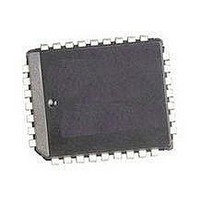
M50FW040K1 STMicroelectronics, M50FW040K1 Datasheet - Page 20

M50FW040K1
Manufacturer Part Number
M50FW040K1
Description
Flash 3.6V 4M (512Kx8)
Manufacturer
STMicroelectronics
Datasheet
1.M50FW040K1.pdf
(41 pages)
Specifications of M50FW040K1
Data Bus Width
8 bit
Memory Type
NOR
Memory Size
4 Mbit
Architecture
Sectored
Interface Type
Firmware Hub
Access Time
11 ns, 50 ns
Supply Voltage (max)
3.6 V
Supply Voltage (min)
3 V
Maximum Operating Current
20 mA
Operating Temperature
+ 70 C
Mounting Style
SMD/SMT
Package / Case
PLCC-32
Organization
512 KB x 8
Lead Free Status / Rohs Status
No
Available stocks
Company
Part Number
Manufacturer
Quantity
Price
Company:
Part Number:
M50FW040K1
Manufacturer:
ST
Quantity:
3 112
Company:
Part Number:
M50FW040K1
Manufacturer:
STM
Quantity:
245
Company:
Part Number:
M50FW040K1
Manufacturer:
QP-SEMI
Quantity:
13
Part Number:
M50FW040K1
Manufacturer:
ST
Quantity:
20 000
Company:
Part Number:
M50FW040K1T
Manufacturer:
TI
Quantity:
125
Part Number:
M50FW040K1T
Manufacturer:
ST
Quantity:
20 000
M50FW040
Table 9. Firmware Hub Register Configuration Map
Table 10. Lock Register Bit Definitions
Note: 1. Applies to Top Block Lock Register (T_BLOCK_LK) and Top Block [-1] Lock Register (T_MINUS01_LK) to Top Block [-7] Lock Reg-
Table 11. General Purpose Inputs Register Definition
Note: 1. Applies to the General Purpose Inputs Register (FGPI-REG).
20/41
T_MINUS01_LK
T_MINUS02_LK
T_MINUS03_LK
T_MINUS04_LK
T_MINUS05_LK
T_MINUS06_LK
T_MINUS07_LK
7-3
Bit
7-5
Bit
2
1
0
T_BLOCK_LK
MANUF_REG
4
3
2
1
0
FGPI_REG
Mnemonic
DEV_REG
Lock-Down
Read-Lock
Write-Lock
Bit Name Value
ister (T_MINUS07_LK).
Bit Name
FGPI4
FGPI3
FGPI2
FGPI1
FGPI0
Top Block Lock Register (Block 7)
Top Block [-1] Lock Register (Block 6)
Top Block [-2] Lock Register (Block 5)
Top Block [-3] Lock Register (Block 4)
Top Block [-4] Lock Register (Block 3)
Top Block [-5] Lock Register (Block 2)
Top Block [-6] Lock Register (Block 1)
Top Block [-7] Lock Register (Block 0)
Firmware Hub (FWH) General Purpose Input Register
Manufacturer Code Register
Device Code Register
‘1’
‘0’
‘1’
‘0’
‘1’
‘0’
Value
Reserved
Bus Read operations in this Block always return 00h.
Bus read operations in this Block return the Memory Array contents. (Default value).
Changes to the Read-Lock bit and the Write-Lock bit cannot be performed. Once a ‘1’ is
written to the Lock-Down bit it cannot be cleared to ‘0’; the bit is always reset to ‘0’ following
a Reset (using RP or INIT) or after power-up.
Read-Lock and Write-Lock can be changed by writing new values to them. (Default value).
Program and Erase operations in this Block will set an error in the Status Register. The
memory contents will not be changed. (Default value).
Program and Erase operations in this Block are executed and will modify the Block contents.
‘1’
‘0’
‘1’
‘0’
‘1’
‘0’
‘1’
‘0’
‘1’
‘0’
Reserved
Input Pin FGPI4 is at V
Input Pin FGPI4 is at V
Input Pin FGPI3 is at V
Input Pin FGPI3 is at V
Input Pin FGPI2 is at V
Input Pin FGPI2 is at V
Input Pin FGPI1 is at V
Input Pin FGPI1 is at V
Input Pin FGPI0 is at V
Input Pin FGPI0 is at V
Register Name
IH
IL
IH
IL
IH
IL
IH
IL
IH
IL
Function
Function
FBD0002h
FBC0002h
FBC0100h
FBC0000h
FBC0001h
FBF0002h
FBE0002h
FBB0002h
FBA0002h
FB90002h
FB80002h
Address
Memory
Default
Value
2Ch
20h
01h
01h
01h
01h
01h
01h
01h
01h
N/A
Access
R/W
R/W
R/W
R/W
R/W
R/W
R/W
R/W
R
R
R


