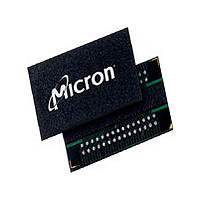
MT46V32M16BN-6:FTR Micron Technology Inc, MT46V32M16BN-6:FTR Datasheet - Page 15

MT46V32M16BN-6:FTR
Manufacturer Part Number
MT46V32M16BN-6:FTR
Description
Manufacturer
Micron Technology Inc
Datasheet
1.MT46V32M16BN-6FTR.pdf
(91 pages)
Specifications of MT46V32M16BN-6:FTR
Lead Free Status / Rohs Status
Compliant
Electrical Specifications – I
Table 6:
PDF: 09005aef80a1d9d4/Source: 09005aef82a95a3a
512Mb_DDR_x4x8x16_D2.fm - 512Mb DDR: Rev. N; Core DDR Rev. B 2/09 EN
Parameter/Condition
Operating one-bank active-precharge current:
t
changing once per clock cycle; Address and control inputs
changing once every two clock cycles
Operating one-bank active-read-precharge current:
Burst = 4;
Address and control inputs
Precharge power-down standby current: All banks idle;
Power-down mode;
Idle standby current: CS# = HIGH; All banks are idle;
t
inputs changing once per clock
and DM
Active power-down standby current: One bank active;
Power-down mode;
Active standby current: CS# = HIGH; CKE = HIGH; One bank
active
inputs changing twice per clock cycle; Address and other
control inputs changing once per clock cycle
Operating burst read current
reads; One bank active; Address and control inputs changing
once per clock cycle;
Operating burst write current: Burst = 2; Continuous burst
writes;
once per clock cycle;
changing twice per clock cycle
Auto refresh burst current:
Self refresh current: CKE ≤ 0.2V
Operating bank interleave read current: Four bank
interleaving READs (burst = 4) with auto precharge,
t
control inputs change only during active READ or WRITE
commands
RC =
CK =
RC = minimum
;
t
t
RC (MIN);
CK (MIN);
t
One bank
RC =
t
RC =
t
I
V
0°C ≤ T
RAS (MAX);
DD
DD
t
t
RC allowed;
t
RC (MIN);
Q = +2.6V ±0.1V, V
CKE = HIGH; Address and other control
Specifications and Conditions (x4, x8)
CK =
active; Address and control inputs changing
t
t
A
t
CK =
CK =
t
CK =
CK =
≤ +70°C; Notes: 1–5, 11, 13, 15, 47; Notes appear on pages 35–40; See also Table 8 on page 17
t
CK (MIN); DQ, DM, and DQS inputs
t
t
t
CK =
t
CK (MIN); CKE = (LOW)
CK (MIN); CKE = LOW
t
CK (MIN); DQ, DM, and DQS inputs
CK (MIN);
t
CK =
changing once per clock cycle
t
CK =
cycle; V
t
CK (MIN); DQ, DM, and DQS
:
t
Burst = 2;
CK (MIN); I
t
CK (MIN); Address and
DD
I
OUT
= +2.6V ±0.1V (-5B); V
IN
= V
= 0mA
t
t
t
Standard
Low power (L)
RFC =
RFC = 7.8µs
RFC = 1.95µs (AT)
DD
REF
Continuous burst
OUT
for DQ, DQS,
= 0mA;
t
RFC (MIN)
15
DD
Q = +2.5V ±0.2V, V
Symbol -5B -6/6T -75E -75Z/-75
I
I
I
I
I
I
I
I
I
DD
DD
DD
DD
DD
I
I
DD
DD
DD
DD
I
I
I
DD
DD
DD
DD
DD
4W
3N
5A
5A
6A
2P
3P
4R
2F
0
1
5
6
7
Micron Technology, Inc., reserves the right to change products or specifications without notice.
155
185
190
195
345
450
55
45
60
11
16
5
5
3
512Mb: x4, x8, x16 DDR SDRAM
130
160
165
175
290
405
45
35
50
10
15
Electrical Specifications – I
DD
5
5
3
= +2.5V ±0.2V (-6, -6T, -75E, -75Z, -75);
130
160
165
155
290
400
45
35
50
10
15
5
5
3
©2000 Micron Technology, Inc. All rights reserved.
115
145
145
135
280
350
40
30
45
10
15
5
5
3
Units
mA
mA
mA
mA
mA
mA
mA
mA
mA
mA
mA
mA
mA
mA
Notes
23, 48
23, 48
24, 33
24, 33
23, 48
28, 50
28, 50
23, 49
51
23
23
50
12
12
DD


