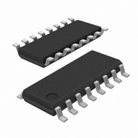
SI3019-F-GSR Silicon Laboratories Inc, SI3019-F-GSR Datasheet - Page 45

SI3019-F-GSR
Manufacturer Part Number
SI3019-F-GSR
Description
IC VOICE DAA GCI/PCM/SPI 16SOIC
Manufacturer
Silicon Laboratories Inc
Datasheet
1.SI3019-F-GSR.pdf
(112 pages)
Specifications of SI3019-F-GSR
Function
Data Access Arrangement (DAA)
Interface
GCI, PCM, SPI
Number Of Circuits
1
Voltage - Supply
3 V ~ 3.6 V
Current - Supply
8.5mA
Operating Temperature
-40°C ~ 85°C
Mounting Type
Surface Mount
Package / Case
16-SOIC (3.9mm Width)
Includes
Line Voltage Monitor, Loop Current Monitor, Overload Detection, Parallel Handset Detection, Polarity Reversal Detection, TIP and
Lead Free Status / RoHS Status
Lead free / RoHS Compliant
Power (watts)
-
Lead Free Status / RoHS Status
Supplier Unconfirmed, Lead free / RoHS Compliant
5.35. SPI Control Interface
The control interface to the Si3050 is a 4-wire interface
modeled on commonly available micro-controller and
serial peripheral devices. The interface consists of four
pins: clock (SCLK), chip select (CS), serial data input
(SDI), and serial data output (SDO). In addition, the
Si3050 includes a serial data through output pin
(SDITHRU) to support daisy chain operation of up to 16
devices. The device can operate with 8-bit and 16-bit
SPI controllers. Each SPI operation consists of a control
byte, an address byte (of which only the six LSBs are
used internally), and either one or two data bytes
depending on the width of the controller. Bytes are
transmitted MSB first.
There are a number of variations of usage on this
four-wire interface as follows:
The bits are defined as follows:
3:0
BRCT
7
6
5
4
Continuous clocking. During continuous clocking,
assertion of the CS pin controls the data transfers.
The CS pin must be asserted before the falling edge
of SCLK on which the first bit of data is expected
during a read cycle, and must remain low for the
7
CID[0:3]
BRCT
R/W
1
0
R/W
6
Indicates a broadcast operation that is intended for all devices in the daisy chain. This is only
valid for write operations as it causes contention on the SDO pin during a read.
Read/Write Bit.
1 = Read operation.
0 = Write operation.
This bit must be 1 at all times.
This bit must be 0 at all times.
This field indicates the channel that is targeted by the operation. The 4-bit channel value is pro-
vided LSB first. The devices reside on the daisy chain such that device 0 is nearest to the con-
troller and device 15 is furthest away in the SDI/SDITHRU chain. See Figure 34.
As the CID information propagates down the daisy chain, each channel decrements the CID by
1. The device that receives a value of 0 in the CID field responds to the SPI transaction. See
Figure 35. If a broadcast to all devices connected to the chain is requested, the CID do not
decrement. In this case, the same 8- or 16-bit data is presented to all channels regardless of
the CID values.
5
1
4
0
CID[0]
3
Rev. 1.31
CID[1]
The SPI state machine resets when the CS pin is
asserted during an operation on an SCLK cycle that is
not a multiple of eight. This provides a mechanism for
the controller to force the state machine to a known
state in the case where the controller and the device are
not synchronized.
The control byte has the following structure and is
presented on the SDI pin MSB first.
2
duration of the 8-bit transfer (command/address or
data), going high after the last rising edge of SCLK
after the transfer.
Clock only during transfer. The clock is active during
the actual byte transfers only. Each byte transfer
consists of eight clock cycles in a return to 1 format.
SDI/SDO wired operation. Independent of the
clocking options described, the SDI and SDO pins
can be treated as two separate lines or wired
together if the master can tri-state its output during
the data byte transfer of a read operation.
CID[2]
Si3050 + Si3018/19
1
CID[3]
0
45


