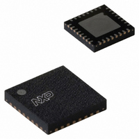
SC16C750BIBS,151 NXP Semiconductors, SC16C750BIBS,151 Datasheet - Page 19

SC16C750BIBS,151
Manufacturer Part Number
SC16C750BIBS,151
Description
IC UART SINGLE W/FIFO 32-HVQFN
Manufacturer
NXP Semiconductors
Type
5 V, 3.3 V and 2.5 V UART with 64-byte FIFOsr
Datasheet
1.SC16C750BIA44518.pdf
(44 pages)
Specifications of SC16C750BIBS,151
Number Of Channels
1, UART
Package / Case
32-VFQFN Exposed Pad
Fifo's
64 Byte
Voltage - Supply
2.5V, 3.3V, 5V
With Auto Flow Control
Yes
With False Start Bit Detection
Yes
With Modem Control
Yes
With Cmos
Yes
Mounting Type
Surface Mount
Data Rate
3 Mbps
Supply Voltage (max)
5.5 V
Supply Voltage (min)
2.25 V
Supply Current
4.5 mA
Maximum Operating Temperature
+ 85 C
Minimum Operating Temperature
- 40 C
Mounting Style
SMD/SMT
Operating Supply Voltage
2.5 V or 3.3 V or 5 V
Lead Free Status / RoHS Status
Lead free / RoHS Compliant
Lead Free Status / RoHS Status
Lead free / RoHS Compliant, Lead free / RoHS Compliant
Other names
568-3285
935276388151
SC16C750BIBS-S
935276388151
SC16C750BIBS-S
NXP Semiconductors
SC16C750B_5
Product data sheet
Table 10.
Table 11.
Bit
2
1
0
FCR[7]
0
0
1
1
Symbol
FCR[3]
(continued)
FCR[2]
FCR[1]
FCR[0]
FIFO Control Register bits description
RCVR trigger levels
FCR[6]
0
1
0
1
Description
Transmit operation in mode ‘1’: When the SC16C750B is in FIFO mode
(FCR[0] = logic 1; FCR[3] = logic 1), the TXRDY pin will be a logic 1 when
the transmit FIFO is completely full. It will be a logic 0 when the FIFO is
emptied.
Receive operation in mode ‘1’: When the SC16C750B is in FIFO mode
(FCR[0] = logic 1; FCR[3] = logic 1) and the trigger level has been reached,
or a Receive Time-Out has occurred, the RXRDY pin will go to a logic 0.
Once activated, it will go to a logic 1 after there are no more characters in
the FIFO.
XMIT FIFO reset.
RCVR FIFO reset.
FIFO enable.
Rev. 05 — 17 October 2008
logic 0 = no FIFO transmit reset (normal default condition)
logic 1 = clears the contents of the transmit FIFO and resets the FIFO
counter logic (the transmit shift register is not cleared or altered). This bit
will return to a logic 0 after clearing the FIFO.
logic 0 = no FIFO receive reset (normal default condition)
logic 1 = clears the contents of the receive FIFO and resets the FIFO
counter logic (the receive shift register is not cleared or altered). This bit
will return to a logic 0 after clearing the FIFO.
logic 0 = disable the transmit and receive FIFO (normal default condition)
logic 1 = enable the transmit and receive FIFO
RX FIFO trigger level (bytes)
16-byte operation
1
4
8
14
5 V, 3.3 V and 2.5 V UART with 64-byte FIFOs
…continued
64-byte operation
1
16
32
56
SC16C750B
© NXP B.V. 2008. All rights reserved.
19 of 44


