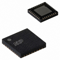
SC16C750BIBS,151 NXP Semiconductors, SC16C750BIBS,151 Datasheet - Page 9

SC16C750BIBS,151
Manufacturer Part Number
SC16C750BIBS,151
Description
IC UART SINGLE W/FIFO 32-HVQFN
Manufacturer
NXP Semiconductors
Type
5 V, 3.3 V and 2.5 V UART with 64-byte FIFOsr
Datasheet
1.SC16C750BIA44518.pdf
(44 pages)
Specifications of SC16C750BIBS,151
Number Of Channels
1, UART
Package / Case
32-VFQFN Exposed Pad
Fifo's
64 Byte
Voltage - Supply
2.5V, 3.3V, 5V
With Auto Flow Control
Yes
With False Start Bit Detection
Yes
With Modem Control
Yes
With Cmos
Yes
Mounting Type
Surface Mount
Data Rate
3 Mbps
Supply Voltage (max)
5.5 V
Supply Voltage (min)
2.25 V
Supply Current
4.5 mA
Maximum Operating Temperature
+ 85 C
Minimum Operating Temperature
- 40 C
Mounting Style
SMD/SMT
Operating Supply Voltage
2.5 V or 3.3 V or 5 V
Lead Free Status / RoHS Status
Lead free / RoHS Compliant
Lead Free Status / RoHS Status
Lead free / RoHS Compliant, Lead free / RoHS Compliant
Other names
568-3285
935276388151
SC16C750BIBS-S
935276388151
SC16C750BIBS-S
NXP Semiconductors
SC16C750B_5
Product data sheet
6.1 Internal registers
The rich feature set of the SC16C750B is available through internal registers. Automatic
hardware flow control, selectable transmit and receive FIFO trigger level, selectable TX
and RX baud rates, modem interface controls, and a sleep mode are some of these
features.
The SC16C750B provides 12 internal registers for monitoring and control. These registers
are shown in
standard 16C550. These registers function as data holding registers (THR/RHR), interrupt
status and control registers (IER/ISR), a FIFO Control Register (FCR), line status and
control registers (LCR/LSR), modem status and control registers (MCR/MSR),
programmable data rate (clock) control registers (DLL/DLM), and a user accessible
Scratchpad Register (SPR). Register functions are more fully described in the following
paragraphs.
Table 3.
[1]
[2]
A2
General register set (THR/RHR, IER/ISR, MCR/MSR, FCR, LSR, SPR)
0
0
0
0
1
1
1
1
Baud rate register set (DLL/DLM)
0
0
These registers are accessible only when LCR[7] is a logic 0.
These registers are accessible only when LCR[7] is a logic 1.
A1
0
0
1
1
0
0
1
1
0
0
Internal registers decoding
Table
A0
0
1
0
1
0
1
0
1
0
1
3. These twelve registers are similar to those already available in the
Rev. 05 — 17 October 2008
READ mode
Receive Holding Register
Interrupt Enable Register
Interrupt Status Register
Line Control Register
Modem Control Register
Line Status Register
Modem Status Register
Scratchpad Register
LSB of Divisor Latch
MSB of Divisor Latch
[2]
5 V, 3.3 V and 2.5 V UART with 64-byte FIFOs
WRITE mode
Transmit Holding Register
Interrupt Enable Register
FIFO Control Register
Line Control Register
Modem Control Register
n/a
n/a
Scratchpad Register
LSB of Divisor Latch
MSB of Divisor Latch
SC16C750B
[1]
© NXP B.V. 2008. All rights reserved.
9 of 44


