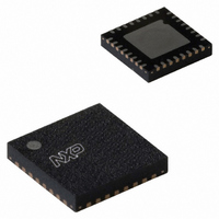
SC16C752BIBS,151 NXP Semiconductors, SC16C752BIBS,151 Datasheet - Page 34

SC16C752BIBS,151
Manufacturer Part Number
SC16C752BIBS,151
Description
IC UART DUAL W/FIFO 32-HVQFN
Manufacturer
NXP Semiconductors
Type
Dual UART with 64-byte FIFOsr
Datasheet
1.SC16C752BIBS151.pdf
(47 pages)
Specifications of SC16C752BIBS,151
Number Of Channels
2, DUART
Package / Case
32-VFQFN Exposed Pad
Features
False-start Bit Detection
Fifo's
64 Byte
Voltage - Supply
2.5V, 3.3V, 5V
With Auto Flow Control
Yes
With False Start Bit Detection
Yes
With Modem Control
Yes
Mounting Type
Surface Mount
Data Rate
5 Mbps
Supply Voltage (max)
5.5 V
Supply Voltage (min)
2.25 V
Supply Current
4.5 mA
Maximum Operating Temperature
+ 85 C
Minimum Operating Temperature
- 40 C
Mounting Style
SMD/SMT
Operating Supply Voltage
2.5 V or 3.3 V or 5 V
Lead Free Status / RoHS Status
Lead free / RoHS Compliant
Lead Free Status / RoHS Status
Lead free / RoHS Compliant, Lead free / RoHS Compliant
Other names
568-3288
935276389151
SC16C752BIBS-S
935276389151
SC16C752BIBS-S
NXP Semiconductors
[5]
[6]
[7]
[8]
11. Dynamic characteristics
Table 26.
T
SC16C752B
Product data sheet
Symbol
t
t
t
t
t
t
t
t
t
t
t
t
t
t
t
t
t
t
t
t
t
t
t
t
t
t
f
t
t
d1
d2
d3
d4
d5
d6
d7
d8
d9
d10
d11
d12
d13
d14
d15
d16
d17
d18
d19
h1
h2
h3
h4
h5
p1
p2
XTAL1
w(RESET)
su1
amb
Except XTAL2, V
These junction temperatures reflect simulated conditions. Absolute maximum junction temperature is 150 °C. The customer is
responsible for verifying junction temperature.
Measurement condition, normal operation other than Sleep mode:
V
recommended operating conditions with divisor of 1.
Sleep mode current might be higher if there is activity on the UART data bus during Sleep mode.
=
CC
−
40
= 3.3 V; T
°
Parameter
IOR delay from chip select
read cycle delay
delay from IOR to data
data disable time
IOW delay from chip select
write cycle delay
delay from IOW to output
delay to set interrupt from modem input
delay to reset interrupt from IOR
delay from stop to set interrupt
delay from IOR to reset interrupt
delay from start to set interrupt
delay from IOW to transmit start
delay from IOW to reset interrupt
delay from stop to set RXRDYn
delay from IOR to reset RXRDYn
delay from IOW to set TXRDYn
delay from start to reset TXRDYn
delay between successive assertion of
IOW and IOR
chip select hold time from IOR
chip select hold time from IOW
data hold time
address hold time
hold time from XTAL1 clock HIGH-to-LOW
transition to IOW or IOR release
clock cycle period
clock cycle period
frequency on pin XTAL1
pulse width on pin RESET
address set-up time
Dynamic characteristics
C to +85
amb
OL
= 25 °C. Full duplex serial activity on all two serial (UART) channels at the clock frequency specified in the
°
= 1 V typical.
C; V
CC
= 2.5 V, 3.3 V
All information provided in this document is subject to legal disclaimers.
±
5 V, 2.2 V and 2.5 V dual UART, 5 Mbit/s (max.), with 64-byte FIFOs
10 % or 5 V
Rev. 6 — 30 November 2010
Conditions
25 pF load
25 pF load
25 pF load
25 pF load
25 pF load
25 pF load
25 pF load
±
10 %, unless specified otherwise.
[2]
[3]
Min
100
10
20
10
25
15
20
10
10
8
0
0
0
0
-
-
-
-
-
-
-
-
-
-
-
-
-
-
-
V
CC
= 2.5 V
24T
16T
1T
1T
Max
100
100
100
RCLK
100
100
100
RCLK
100
100
77
15
RCLK
RCLK
20
48
-
-
-
-
-
-
-
-
-
-
-
-
-
[1]
[1]
[1]
[1]
SC16C752B
V
Min
CC
20
10
25
15
20
40
0
8
0
0
0
6
6
0
-
-
-
-
-
-
-
-
-
-
-
-
-
-
-
= 3.3 V or 5 V Unit
© NXP B.V. 2010. All rights reserved.
24T
16T
1T
1T
Max
RCLK
RCLK
100
15
24
26
33
24
29
RCLK
70
75
70
RCLK
20
80
-
-
-
-
-
-
-
-
-
-
-
-
-
[1]
[1]
[1]
[1]
34 of 47
ns
ns
ns
ns
ns
ns
ns
ns
ns
ns
ns
s
ns
ns
s
ns
s
ns
ns
s
ns
ns
ns
ns
ns
ns
ns
MHz
ns


