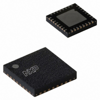
SC16C2550BIBS,151 NXP Semiconductors, SC16C2550BIBS,151 Datasheet - Page 25

SC16C2550BIBS,151
Manufacturer Part Number
SC16C2550BIBS,151
Description
IC UART DUAL W/FIFO 32-HVQFN
Manufacturer
NXP Semiconductors
Type
5 V, 3.3 V and 2.5 V dual UART, 5 Mbit/s with 16-byte FIFOsr
Datasheet
1.SC16C2550BIA44518.pdf
(43 pages)
Specifications of SC16C2550BIBS,151
Number Of Channels
2, DUART
Package / Case
32-VFQFN Exposed Pad
Features
False-start Bit Detection
Fifo's
16 Byte
Voltage - Supply
3.5 V ~ 4.5 V
With Auto Flow Control
Yes
With False Start Bit Detection
Yes
With Modem Control
Yes
With Cmos
Yes
Mounting Type
Surface Mount
Data Rate
5 Mbps
Supply Voltage (max)
5.5 V
Supply Voltage (min)
2.25 V
Supply Current
4.5 mA
Maximum Operating Temperature
+ 85 C
Minimum Operating Temperature
- 40 C
Mounting Style
SMD/SMT
Operating Supply Voltage
2.5 V or 3.3 V or 5 V
Lead Free Status / RoHS Status
Lead free / RoHS Compliant
Lead Free Status / RoHS Status
Lead free / RoHS Compliant, Lead free / RoHS Compliant
Other names
568-3259
935280309151
SC16C2550BIBS-S
935280309151
SC16C2550BIBS-S
Available stocks
Company
Part Number
Manufacturer
Quantity
Price
Company:
Part Number:
SC16C2550BIBS,151
Manufacturer:
NXP
Quantity:
1 861
NXP Semiconductors
8. Limiting values
Table 23.
In accordance with the Absolute Maximum Rating System (IEC 60134).
9. Static characteristics
Table 24.
T
[1]
SC16C2550B_5
Product data sheet
Symbol
V
V
T
T
P
Symbol Parameter
V
V
V
V
V
V
I
I
I
C
LIL
L(clk)
CC
amb
amb
stg
CC
n
tot
IL(clk)
IH(clk)
IL
IH
OL
OH
i
/pack
Except XTAL2, V
= 40 C to +85 C; tolerance of V
clock LOW-level input voltage
clock HIGH-level input voltage
LOW-level input voltage
HIGH-level input voltage
LOW-level output voltage
HIGH-level output voltage
LOW-level input leakage current
clock leakage current
supply current
input capacitance
Limiting values
Static characteristics
Parameter
supply voltage
voltage on any other pin
operating temperature
storage temperature
total power dissipation per package
OL
= 1 V typical.
CC
10 %; unless otherwise specified.
Conditions
except X1 clock
except X1 clock
on all outputs
I
(data bus)
I
(other outputs)
I
(data bus)
I
(other outputs)
f = 5 MHz
OH
OH
OH
OH
5 V, 3.3 V and 2.5 V dual UART, 5 Mbit/s (max.), with 16-byte FIFOs
I
(data bus)
I
(other outputs)
I
(data bus)
I
(other outputs)
OL
OL
OL
OL
= 5 mA
= 1 mA
= 800 A
= 400 A
Rev. 05 — 12 January 2009
= 5 mA
= 4 mA
= 2 mA
= 1.6 mA
Conditions
at D7 to D0 pins
at input only pins
[1]
1.85
1.85
Min
V
1.8
1.6
0.3
0.3
-
-
-
-
-
-
-
-
-
-
CC
= 2.5 V
+0.45
+0.65
Max
V
0.4
0.4
3.5
10
30
5
CC
-
-
-
-
-
-
-
Min
-
GND
GND
-
40
65
Min
V
2.4
2.0
2.0
0.3
0.3
-
-
-
-
-
-
-
-
-
-
-
CC
0.3
0.3
= 3.3 V
SC16C2550B
Max
+0.6
+0.8
V
0.4
4.5
10
30
5
CC
-
-
-
-
-
-
-
-
Max
7
V
5.3
+85
+150
500
CC
+ 0.3
Min
V
© NXP B.V. 2009. All rights reserved.
3.0
2.2
2.4
0.5
0.5
-
-
-
-
-
-
-
-
-
-
-
CC
= 5.0 V
Max
+0.6
+0.8
V
0.4
4.5
10
30
5
CC
-
-
-
-
-
-
-
-
Unit
V
V
V
mW
C
C
25 of 43
Unit
V
V
V
V
V
V
V
V
V
V
V
V
mA
pF
A
A


