SC28L91A1B,551 NXP Semiconductors, SC28L91A1B,551 Datasheet - Page 9
SC28L91A1B,551
Manufacturer Part Number
SC28L91A1B,551
Description
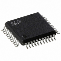
IC UART SINGLE W/FIFO 44-PQFP
Manufacturer
NXP Semiconductors
Series
IMPACTr
Type
Single Channel UARTr
Datasheet
1.SC28L91A1A529.pdf
(43 pages)
Specifications of SC28L91A1B,551
Number Of Channels
1, UART
Package / Case
44-MQFP, 44-PQFP
Features
False-start Bit Detection
Fifo's
16 Byte
Voltage - Supply
3.3V, 5V
With Auto Flow Control
Yes
With False Start Bit Detection
Yes
With Modem Control
Yes
With Cmos
Yes
Mounting Type
Surface Mount
Data Rate
0.2304 MBd
Supply Voltage (max)
5.5 V
Supply Voltage (min)
3 V
Supply Current
25 mA
Maximum Operating Temperature
+ 85 C
Minimum Operating Temperature
- 40 C
Mounting Style
SMD/SMT
Operating Supply Voltage
3.3 V or 5 V
Lead Free Status / RoHS Status
Lead free / RoHS Compliant
Lead Free Status / RoHS Status
Lead free / RoHS Compliant, Lead free / RoHS Compliant
Other names
568-1187
935267419551
SC28L91A1B-S
935267419551
SC28L91A1B-S
Available stocks
Company
Part Number
Manufacturer
Quantity
Price
Company:

Part Number:
SC28L91A1B,551
Manufacturer:
NXP Semiconductors
Quantity:
10 000


Philips Semiconductors
PIN CONFIGURATION FOR 68XXX BUS INTERFACE (MOTOROLA )
2004 Oct 21
Symbol
I/M
D0–D7
CEN
R/WN
IACKN
DACKN
A0–A3
RESETN
INTRN
X1/CLK
X2
RxD
TxD
OP0
OP1
OP2
OP3
OP4
OP5
OP6
OP7
IP0
IP1
IP2
IP3
IP4
IP5
V
GND
CC
3.3 V or 5.0 V Universal Asynchronous
Receiver/Transmitter (UART)
Pin
type
I
I/O
I
I
I
O
I
I
O
I
O
I
O
O
O
O
O
O
O
O
O
I
I
I
I
I
I
Pwr
Pwr
Input 4: General purpose input or receiver external clock input (RxC). When the external clock is used by the receiver,
Input 3: General purpose input or transmitter external clock input (TxC). When the external clock is used by the trans-
Name and function
Bus Configuration: When low configures the bus interface to the Conditions shown in this table.
Data Bus: Bi-directional 3-State data bus used to transfer commands, data and status between the UART and the
CPU. D0 is the least significant bit.
Chip Enable: Active-Low input signal. When Low, data transfers between the CPU and the UART are enabled on
D0–D7 as controlled by the R/WN and A0–A3 inputs. When High, places the D0–D7 lines in the 3-State condition.
Read/Write: Input Signal. When CEN is low R/WN high input indicates a read cycle; when low indicates a write cycle.
Interrupt Acknowledge: Active low input indicating an interrupt acknowledge cycle. Usually asserted by the CPU in
response to an interrupt request. When asserted places the interrupt vector on the bus and asserts DACKN.
Data Transfer Acknowledge: A3-State active-low output asserted in a write, read, or interrupt acknowledge cycle to
indicate proper transfer of data between the CPU and the UART.
Address Inputs: Select the UART internal registers and ports for read/write operations.
Reset: A low level clears internal registers (SRA, SRB, IMR, ISR, OPR, OPCR), puts OP0–OP7 in the High state,
stops the counter/timer, and puts the Channel in the inactive state, with the TxD outputs in the mark (High) state. Sets
MR pointer to MR1. See Figure 4
Interrupt Request: Active-Low, open-drain, output which signals the CPU that one or more of the eight maskable
interrupting conditions are true. This pin requires a pullup.
Crystal 1: Crystal or external clock input. A crystal or clock of the specified limits must be supplied at all times. When
a crystal is used, a capacitor must be connected from this pin to ground (see Figure 11).
Crystal 2: Connection for other side of the crystal. When a crystal is used, a capacitor must be connected from this
pin to ground (see Figure 11). If X1/CLK is driven from an external source, this pin must be left open.
Receiver Serial Data Input: The least significant bit is received first. “Mark” is High, “space” is Low.
Transmitter Serial Data Output: The least significant bit is transmitted first. This output is held in the ‘mark’ condition
when the transmitter is disabled, idle, or when operating in local loop back mode. ‘Mark’ is High; ‘space’ is Low.
Output 0: General purpose output or request to send (RTSAN, active-Low). Can be deactivated automatically on
receive or transmit.
Output 1: General-purpose output.
Output 2: General purpose output or transmitter 1X or 16X clock output, or receiver 1X clock output.
Output 3: General purpose output.
Output 4: General purpose output or open-drain, active-Low, RxA interrupt ISR [1] output. DMA Control
Output 5: General-purpose output.
Output 6: General purpose output or open-drain, active-Low, TxA interrupt ISR[0] output. DMA Control
Output 7: General-purpose output.
Input 0: General purpose input or clear to send active-Low input (CTSAN). Has Change of State Dector.
Input 1: General purpose input. Has Change of State Dector.
Input 2: General-purpose input or counter/timer external clock input. Has Change of State Dector.
mitter, the transmitted data is clocked on the falling edge of the clock. Has Change of State Dector.
the received data is sampled on the rising edge of the clock.
Input 5: General purpose input.
Power Supply: +3.3 or +5V supply input 10%
Ground
9
SC28L91
Product data sheet
Related parts for SC28L91A1B,551
Image
Part Number
Description
Manufacturer
Datasheet
Request
R

Part Number:
Description:
NXP Semiconductors designed the LPC2420/2460 microcontroller around a 16-bit/32-bitARM7TDMI-S CPU core with real-time debug interfaces that include both JTAG andembedded trace
Manufacturer:
NXP Semiconductors
Datasheet:

Part Number:
Description:
NXP Semiconductors designed the LPC2458 microcontroller around a 16-bit/32-bitARM7TDMI-S CPU core with real-time debug interfaces that include both JTAG andembedded trace
Manufacturer:
NXP Semiconductors
Datasheet:
Part Number:
Description:
NXP Semiconductors designed the LPC2468 microcontroller around a 16-bit/32-bitARM7TDMI-S CPU core with real-time debug interfaces that include both JTAG andembedded trace
Manufacturer:
NXP Semiconductors
Datasheet:
Part Number:
Description:
NXP Semiconductors designed the LPC2470 microcontroller, powered by theARM7TDMI-S core, to be a highly integrated microcontroller for a wide range ofapplications that require advanced communications and high quality graphic displays
Manufacturer:
NXP Semiconductors
Datasheet:
Part Number:
Description:
NXP Semiconductors designed the LPC2478 microcontroller, powered by theARM7TDMI-S core, to be a highly integrated microcontroller for a wide range ofapplications that require advanced communications and high quality graphic displays
Manufacturer:
NXP Semiconductors
Datasheet:
Part Number:
Description:
The Philips Semiconductors XA (eXtended Architecture) family of 16-bit single-chip microcontrollers is powerful enough to easily handle the requirements of high performance embedded applications, yet inexpensive enough to compete in the market for hi
Manufacturer:
NXP Semiconductors
Datasheet:
Part Number:
Description:
The XA-S3 device is a member of Philips Semiconductors? XA(eXtended Architecture) family of high performance 16-bitsingle-chip microcontrollers
Manufacturer:
NXP Semiconductors
Datasheet:

Part Number:
Description:
The NXP BlueStreak LH75401/LH75411 family consists of two low-cost 16/32-bit System-on-Chip (SoC) devices
Manufacturer:
NXP Semiconductors
Datasheet:
Part Number:
Description:
The NXP LPC3130/3131 combine an 180 MHz ARM926EJ-S CPU core, high-speed USB2
Manufacturer:
NXP Semiconductors
Datasheet:
Part Number:
Description:
The NXP LPC3141 combine a 270 MHz ARM926EJ-S CPU core, High-speed USB 2
Manufacturer:
NXP Semiconductors
Part Number:
Description:
The NXP LPC3143 combine a 270 MHz ARM926EJ-S CPU core, High-speed USB 2
Manufacturer:
NXP Semiconductors

Part Number:
Description:
The NXP LPC3152 combines an 180 MHz ARM926EJ-S CPU core, High-speed USB 2
Manufacturer:
NXP Semiconductors
Part Number:
Description:
The NXP LPC3154 combines an 180 MHz ARM926EJ-S CPU core, High-speed USB 2
Manufacturer:
NXP Semiconductors

Part Number:
Description:
Standard level N-channel enhancement mode Field-Effect Transistor (FET) in a plastic package using NXP High-Performance Automotive (HPA) TrenchMOS technology
Manufacturer:
NXP Semiconductors
Datasheet: