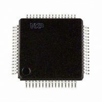
SC16C654BIBM,151 NXP Semiconductors, SC16C654BIBM,151 Datasheet - Page 13

SC16C654BIBM,151
Manufacturer Part Number
SC16C654BIBM,151
Description
IC UART QUAD W/FIFO 64-LQFP
Manufacturer
NXP Semiconductors
Datasheet
1.SC16C654BIBS551.pdf
(58 pages)
Specifications of SC16C654BIBM,151
Features
False-start Bit Detection
Number Of Channels
4, QUART
Fifo's
64 Byte
Voltage - Supply
2.5V, 3.3V, 5V
With Auto Flow Control
Yes
With Irda Encoder/decoder
Yes
With False Start Bit Detection
Yes
With Modem Control
Yes
With Cmos
Yes
Mounting Type
Surface Mount
Package / Case
64-LQFP
Lead Free Status / RoHS Status
Lead free / RoHS Compliant
Other names
568-3278
935279068151
SC16C654BIBM-S
935279068151
SC16C654BIBM-S
Available stocks
Company
Part Number
Manufacturer
Quantity
Price
Company:
Part Number:
SC16C654BIBM,151
Manufacturer:
NXP Semiconductors
Quantity:
10 000
Philips Semiconductors
Table 2:
9397 750 14965
Product data sheet
Symbol
RIA
RIB
RIC
RID
RTSA
RTSB
RTSC
RTSD
R/W
RXA
RXB
RXC
RXD
RXRDY
TXA
TXB
TXC
TXD
Pin
PLCC68 LQFP64 HVQFN48 LFBGA6
8
28
42
62
14
22
48
56
18
7
29
41
63
38
17
19
51
53
Pin description
63
19
30
50
5
13
36
44
-
62
20
29
51
-
8
10
39
41
…continued
-
-
23
-
3
11
29
-
7
48
13
22
38
-
6
8
32
34
4
A2
J3
K8
A9
C2
H2
H9
C10
-
A3
K3
J8
B8
-
E2
F2
F10
E10
5 V, 3.3 V and 2.5 V quad UART, 5 Mbit/s (max.) with 64-byte FIFOs
Rev. 02 — 20 June 2005
Type Description
I
O
I
I
O
O
Ring Indicator (active LOW). These inputs are associated
with individual UART channels, A through D. A logic 0 on this
pin indicates the modem has received a ringing signal from
the telephone line. A logic 1 transition on this input pin will
generate an interrupt.
Request to Send (active LOW). These outputs are
associated with individual UART channels, A through D. A
logic 0 on the RTS pin indicates the transmitter has data
ready and waiting to send. Writing a logic 1 in the modem
control register MCR[1] will set this pin to a logic 0,
indicating data is available. After a reset this pin will be set to
a logic 1. This pin only affects the transmit and receive
operations when Auto RTS function is enabled via the
Enhanced Feature Register (EFR[6]) for hardware flow
control operation.
Read/Write strobe. This function is associated with the
68 mode only. This pin provides the combined functions for
Read or Write strobes.
Logic 1 = Read from UART register selected by CS and
A[0:4].
Logic 0 = Write to UART register selected by CS and A[0:4].
Receive data input RXA-RXD. These inputs are associated
with individual serial channel data to the
SC16C654B/654DB. The RX signal will be a logic 1 during
reset, idle (no data), or when the transmitter is disabled.
During the local loop-back mode, the RX input pin is
disabled and TX data is connected to the UART RX input
internally.
Receive Ready (active LOW). This function is associated
with 68-pin package only. RXRDY contains the wire-ORed
status of all four receive channel FIFOs, RXRDYA-RXRDYD.
A logic 0 indicates receive data ready status, that is, the
RHR is full, or the FIFO has one or more RX characters
available for unloading. This pin goes to a logic 1 when the
FIFO/RHR is empty, or when there are no more characters
available in either the FIFO or RHR. Individual channel RX
status is read by examining individual internal registers via
CS and A[0:4] pin functions.
Transmit data A, B, C, D. These outputs are associated
with individual serial transmit channel data from the
SC16C654B/654DB. The TX signal will be a logic 1 during
reset, idle (no data), or when the transmitter is disabled.
During the local loop-back mode, the TX output pin is
disabled and TX data is internally connected to the UART
RX input.
SC16C654B/654DB
© Koninklijke Philips Electronics N.V. 2005. All rights reserved.
13 of 58


