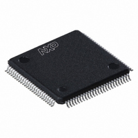
SC28L198A1BE,557 NXP Semiconductors, SC28L198A1BE,557 Datasheet - Page 27

SC28L198A1BE,557
Manufacturer Part Number
SC28L198A1BE,557
Description
IC UART OCTAL W/FIFO 100-LQFP
Manufacturer
NXP Semiconductors
Datasheet
1.SC28L198A1BE557.pdf
(57 pages)
Specifications of SC28L198A1BE,557
Features
False-start Bit Detection
Number Of Channels
8
Fifo's
16 Byte
Voltage - Supply
3.3V, 5V
With Auto Flow Control
Yes
With False Start Bit Detection
Yes
With Modem Control
Yes
With Cmos
Yes
Mounting Type
Surface Mount
Package / Case
100-LQFP
Lead Free Status / RoHS Status
Lead free / RoHS Compliant
Other names
568-1210
935262731557
SC28L198A1BE
935262731557
SC28L198A1BE
Available stocks
Company
Part Number
Manufacturer
Quantity
Price
Company:
Part Number:
SC28L198A1BE,557
Manufacturer:
NXP Semiconductors
Quantity:
10 000
Philips Semiconductors
Table 22. XISR – Xon–Xoff Interrupt Status Register
XISR[7:6] – Received X Character Status. This field can be read to
determine if the receiver has encountered an Xon or Xoff character
in the incoming data stream. These bits are maintained until a read
of the XISR. The field is updated by X character reception
regardless of the state of MR0(7, 3:2) or IMR(4). The field can
therefore be used as a character detector for the bit patterns stored
in the Xon and Xoff Character Registers.
XISR[5:4] – Automatic transmission Status. This field indicates the
last flow control character sent in the Auto Receiver flow control
mode. If Auto Receiver mode has not been enabled, this field will
always read b’00. It will likewise reset to b’00 if MR0(3) is reset. If
the Auto Receiver mode is exited while this field reads b’10, it is the
user’s responsibility to transmit an Xon, when appropriate.
XISR[3:2] – TxD flow Status. This field tracks the transmitter’s flow
status as follows:
XISR[1:0] – TxD character Status. This field allows determination of
the type of character being transmitted. If XISR(1:0) is b’01, the
channel is waiting for a data character to transfer from the TxFIFO.
This condition will only occur for a bit time after an Xon or Xoff
character transmission unless the TxFIFO is empty.
Table 26. BRGTCR – BRG Timer Control Register (BRGTCR)
Start/Stop control and clock select register for the two BRG
counters. The clock selection is for the input to the counters. It is
that clock divided by the number represented by the BRGTU and
BRGTL the will be used as the 16x clock for the receivers and
transmitters. When the BRG timer Clock is selected for the
2006 Aug 10
Bits 7:6
Received X Character Sta-
tus
00 – none
01 – Xoff received
10 – Xon received
11 – both received
Bit 7
BRGTCR b, Register control
0 – Resets the timer register and
holds it stopped
1 – Allows the timer register to
run.
10 – re–enabled. The transmitter had been halted and restarted.
Octal UART for 3.3 V and 5 V supply voltage
00 – normal. The flow control is under host control.
01 – TxD halt pending. After the current character finishes the
transmitter will stop. The status will then change to b’00.
It is sending data characters. After a read of the XISR, it will
return to ”normal” status.
11 – disabled. The transmitter is flow controlled.
Bits 5:4
Automatic X Character transmis-
sion status
00 – none
01 – Xon transmitted
10 – Xoff transmitted
11 – Illegal, does not occur
Bit 6:4
BRGTCR b, Clock selection
000 – Sclk / 16
001 – Sclk / 32
010 – Sclk/ 64
011 – Sclk / 128
100 – X1
101 – X1 / 2
110 – I/O1b
111 – G
IN
(1)
Bits 3:2
TxD flow status
00 – normal
01 – TxD halt pending
10 – re–enabled
11 – flow disabled
27
Bit 3
BRGTCR a, Register control
0 – Resets the timer register and
holds it stopped.
1 – Allows the timer register to
run.
Table 23. WDTRCR – Watch-dog Timer Enable
This register enables the watch-dog Timer for each of the 8
receivers on the Octal UART.
Table 24. BRGTRU
This is the upper byte of the 16 bit value used by the BRG timer in
generating a baud rate clock
Table 25. BRGTRL
This is the lower byte of the 16 bit value used by the BRG timer in
generating a baud rate clock.
receiver(s) or transmitter(s) the receivers and transmitters will
consider it as a 16x clock and further device it by 16. In other words
the receivers and transmitters will always be in the 16x ode of
operation when the internal BRG timer is selected for their clock.
Bit 7
WDT
h
1 on
0 off
Bits 7:0
8 MSB of the BRG Timer divisor.
Bits 7:0
8 LSB of the BRG Timer divisor.
Bit 6
WDT
g
1 on
0 off
Register
Registers, Upper
Registers, Lower
Bit 5
WDT
f
1 on
0 off
–
Bit 4
WDT
e
1 on
0 off
–
Bits 1:0
TxD character status
00 – normal TxD data
01 – wait on normal data
10 – Xoff in pending
11 – Xon in pending
BRG Timer Reload
BRG Timer Reload
Bit 2:0
BRGTCR a, Clock selection
000 – Sclk / 16
001 – Sclk / 32
010 – Sclk / 64
011 – Sclk / 128
100 – X1
101 – X1 / 2
110 – I/O1a
111 – G
Bit 3
WDT
d
1 on
0 off
IN
(0)
Bit 2
WDT
c
1 on
0 off
SC28L198
Product data sheet
Bit 1
WDT
b
1 on
0 off
Bit 0
WDT
a
1 on
0 off


