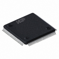
SC28L198A1BE,557 NXP Semiconductors, SC28L198A1BE,557 Datasheet - Page 44

SC28L198A1BE,557
Manufacturer Part Number
SC28L198A1BE,557
Description
IC UART OCTAL W/FIFO 100-LQFP
Manufacturer
NXP Semiconductors
Datasheet
1.SC28L198A1BE557.pdf
(57 pages)
Specifications of SC28L198A1BE,557
Features
False-start Bit Detection
Number Of Channels
8
Fifo's
16 Byte
Voltage - Supply
3.3V, 5V
With Auto Flow Control
Yes
With False Start Bit Detection
Yes
With Modem Control
Yes
With Cmos
Yes
Mounting Type
Surface Mount
Package / Case
100-LQFP
Lead Free Status / RoHS Status
Lead free / RoHS Compliant
Other names
568-1210
935262731557
SC28L198A1BE
935262731557
SC28L198A1BE
Available stocks
Company
Part Number
Manufacturer
Quantity
Price
Company:
Part Number:
SC28L198A1BE,557
Manufacturer:
NXP Semiconductors
Quantity:
10 000
1. Timing is illustrated and referenced with respect to W–RN and CEN inputs. Internal read and write activities are controlled by the Sclk as it
2. The minimum time before the rising edge of the next C2 time to stop the next bus cycle. CEN must return high after midpoint of C4 time and
3. Delay is from CEN high in Async mode to IRQN inactive, from end of C4 to IRQN inactive in Sync mode.
4. The minimum frequency values are not tested, but are guaranteed by design.
5. 1MHz specification is for crystal operation.
Philips Semiconductors
AC ELECTRICAL CHARACTERISTICS FOR COMMERCIAL AND INDUSTRIAL (5 V) (Continued)
V
NOTES:
2006 Aug 10
Sclk Timing
t
t
F
t/
X1/X2 Communication Crystal Clock
Fx1
X1 L / H
T/RFx1
Counter/Timer Baud Rate Clock (External Clock Input)
FC/T
TC/TLH
TC/TO
DTACK Timing
DAKdly
DAKdlya
DAKdlys
I/O Port External Clock
tgpirtx
Gout Timing
GPOtdd
CC
sclkl
sclkh
sclk
RFsck
Octal UART for 3.3 V and 5 V supply voltage
SYMBOL
generates the several “C” timing as shown in the timing diagrams.
before the C2 time of the next cycle.
= 5.0 volts
5
4
10 %; T
FIG#
A
= –40 C to +85 C; unless otherwise specified
Min low time at V
Min high time at V
Sclk frequency
Sclk rise and fall time (0.8 to 2.0Volts)
X1 Low / High time
X1 Rise and Fall time
Clock frequency
C/T high and low time
Delay C/T clock external to output pin
DACK low from Sclk C4 rising edge
DACK high from CEN high (Async)
DACK high from C4 end rising edge (Sync)
GPI to Rx/Tx clock out
RxD setup to I/OP rising edge 1X mode
I/OP falling edge to TxD out 1X mode
GPO valid after write to GPOR
X1 clock frequency
IL
IH
(0.8V)
(2.0V)
PARAMETER
44
MIN
0.1
11
11
32
15
20
1
0
LIMITS
3.6864
TYP
135
100
11
48
10
11
11
32
32
5
5
2
SC28L198
MAX
8.0
Product data sheet
33
10
60
18
20
20
50
60
3
8
UNIT
MHz
MHz
MHz
ns
ns
ns
ns
ns
ns
ns
ns
ns
ns
ns
ns
ns
ns


