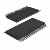
SC28L202A1DGG,118 NXP Semiconductors, SC28L202A1DGG,118 Datasheet - Page 51

SC28L202A1DGG,118
Manufacturer Part Number
SC28L202A1DGG,118
Description
IC UART DUAL W/FIFO 56-TSSOP
Manufacturer
NXP Semiconductors
Series
IMPACTr
Datasheet
1.SC28L202A1DGG118.pdf
(77 pages)
Specifications of SC28L202A1DGG,118
Features
False-start Bit Detection
Number Of Channels
2, DUART
Fifo's
256 Byte
Voltage - Supply
3.3V, 5V
With Parallel Port
Yes
With Auto Flow Control
Yes
With False Start Bit Detection
Yes
With Modem Control
Yes
With Cmos
Yes
Mounting Type
Surface Mount
Package / Case
56-TFSOP (0.240", 6.10mm Width)
Lead Free Status / RoHS Status
Lead free / RoHS Compliant
Other names
935276109118
SC28L202A1DGG-T
SC28L202A1DGG-T
SC28L202A1DGG-T
SC28L202A1DGG-T
Available stocks
Company
Part Number
Manufacturer
Quantity
Price
Company:
Part Number:
SC28L202A1DGG,118
Manufacturer:
EPCOS
Quantity:
12 000
Philips Semiconductors
CR A and B Command Register
CR, one for each channel, controls the channel commands and enables/disables the receiver and transmitter. Commands may be to the upper
and lower four bits in the same bus cycle. If both enable and disable bits are set to 1 in the lower four bits a disable will result.
CR Command Register
NOTE: Access to the miscellaneous commands should be separated by 3 X1 clock edges. A disabled transmitter cannot be loaded.
COMMAND REGISTER TABLE A and B
Commands 0xE, 0xF (marked with *) are global and exist only in channel A’s register space.
It is used in either character or block mode. In block mode it would
normally be used after the block is read.
2005 Nov 01
CR A &CR B
Channel Command Code
CR[7:4]
0000
0001
0010
0011
0100
0101
0110
0111
0000 No command.
0001 set MR pointer to 1
0010 Reset receiver. Immediately resets the receiver as if
hardware reset had been applied. The receiver is reset and the
FIFO pointer is reset to the first location effectively discarding all
unread characters in the FIFO.
0011 Reset transmitter. Immediately resets the transmitter as if a
hardware reset had been applied. The transmitter is reset and the
FIFO pointer is reset to the first location effectively discarding all
untransmitted characters in the FIFO.
0100 Reset error status. Clears the received break, parity error,
framing error, and overrun error bits in the status register
(SR[7:4]). I
0101 Reset break change interrupt. Causes the break detect
change bit in the interrupt status register (ISR[2]) to be cleared to
zero.
0110 Start break. Forces the TxD output low (spacing). If the
transmitter is empty, the start of the break condition will be
delayed up to two bit times. If the transmitter is active and the
TxFIFO is empty then the break begins when transmission of the
current character is completed. If there are characters in the
TxFIFO, the start of break is delayed until all characters presently
in the TxFIFO and any subsequent characters loaded have been
transmitted. (Tx Idle must be true before break begins).
Dual UART
Bit 7
MISCELLANEOUS COMMANDS
See Text of Channel Command Register
Channel Command
Description
NOP
Set MR pointer to 1
Reset Receiver
Reset Transmitter
Reset Error Status
Reset Break Change Interrupt
Begin Transmit Break
End Transmit Break
BIT 6
BIT 5
BIT 4
Channel Command Code
CR[7:4]
1000
1001
1010
1011
1100
1101
1110
1111
45
BIT 3
Disable Tx
1 = Yes
0 = No
The transmitter must be enabled to start a break.
0111 Stop break. The TxD line will go high (marking) within two bit
times. TxD will remain high for one bit time before the next
character is transmitted.
1000 Assert RTSN. Causes the RTSN output to be asserted (low).
1001 Negate RTSN. Causes the RTSN output to be negated
(high).
1010 Set C/T Receiver time out mode on. The receiver in this
channel will restart the C/T as reach receive character is
transferred from the shift register to the RxFIFO. The C/T is
placed in the Counter Mode, the Start/Stop Counter commands
are disabled, the counter is stopped and the Counter Ready bit,
ISR(3), is reset.
1011 Set MR Pointer to 0
1100 Set C/T Receiver time out mode off
1101 Block error status accumulation on FIFO entry. Allows the
‘received break’, ‘framing error’ and ‘parity error’ bits to be set as
the received character is loaded to the RxFIFO. (normally these
bits are set on reading of the data from the RxFIFO) Setting this
mode can give information about error data up to 256 bytes earlier
than the normal mode. However it clouds the ability to know
precisely which byte(s) are in error.
1110 Power Down Mode On
1111 Disable Power Down Mode
NOTE: The two commands above actually reset and set,
respectively, the I/O0 B or I/O1 B pin associated WITH the
OPR register.
BIT 2
Enable Tx
1 = Yes
0 = No
Channel Command
Description
Assert RTSN (I/O0 B or I/O1 B)
Negate RTSN (I/O0 B or I/O1 B)
Set C/T Receiver time–out mode on
Set MR pointer to 0
Set C/T Receiver time–out mode off
Block Error Status on RxFIFO load
Power Down Mode On
Disable Power Down Mode
BIT 1
Disable Rx
1 = Yes
0 = No
SC28L202
Product data sheet
BIT 0
Enable Rx
1 = Yes
0 = No


